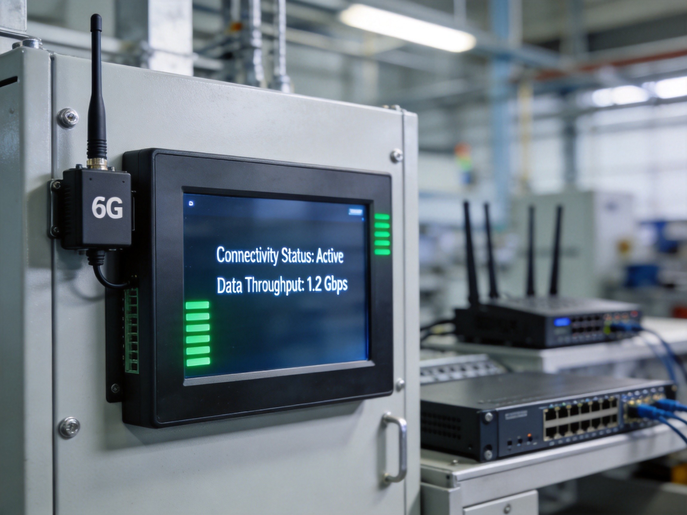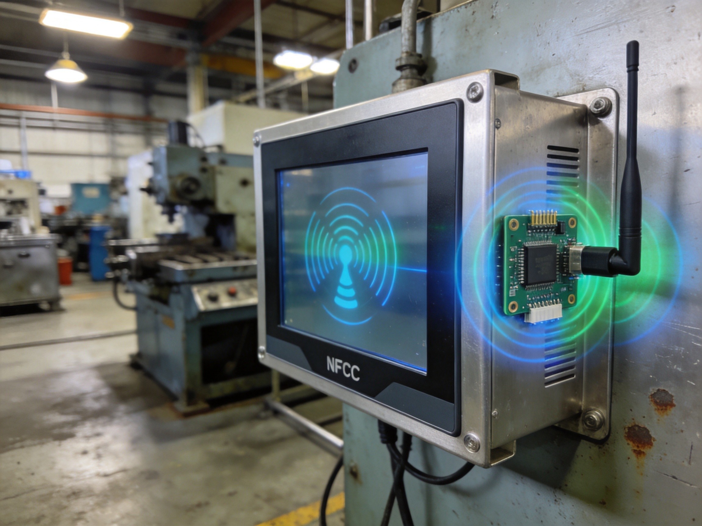
Semiconductor fabrication represents one of the most demanding computing environments in modern industry. Inside a wafer fab, every variable matters: sub-micron particle counts, temperature fluctuations measured in tenths of a degree, vibration levels that could distort lithography alignment. The computers that monitor these processes must operate flawlessly while being sources of zero contamination. Industrial panel PCs in cleanroom environments face requirements far beyond standard industrial ruggedness. With SEMICON Taiwan 2026 highlighting accelerating investment in smart factory infrastructure and 300-millimeter fab equipment spending projected to surpass 150 billion dollars for the first time in 2027, the demand for cleanroom-qualified computing hardware has never been stronger.
Cleanroom Classification and Panel PC Requirements
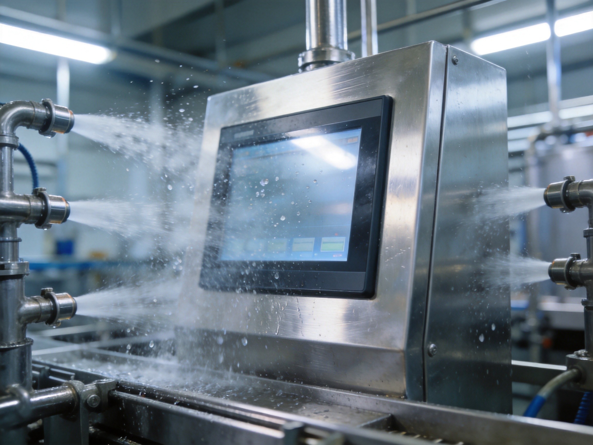
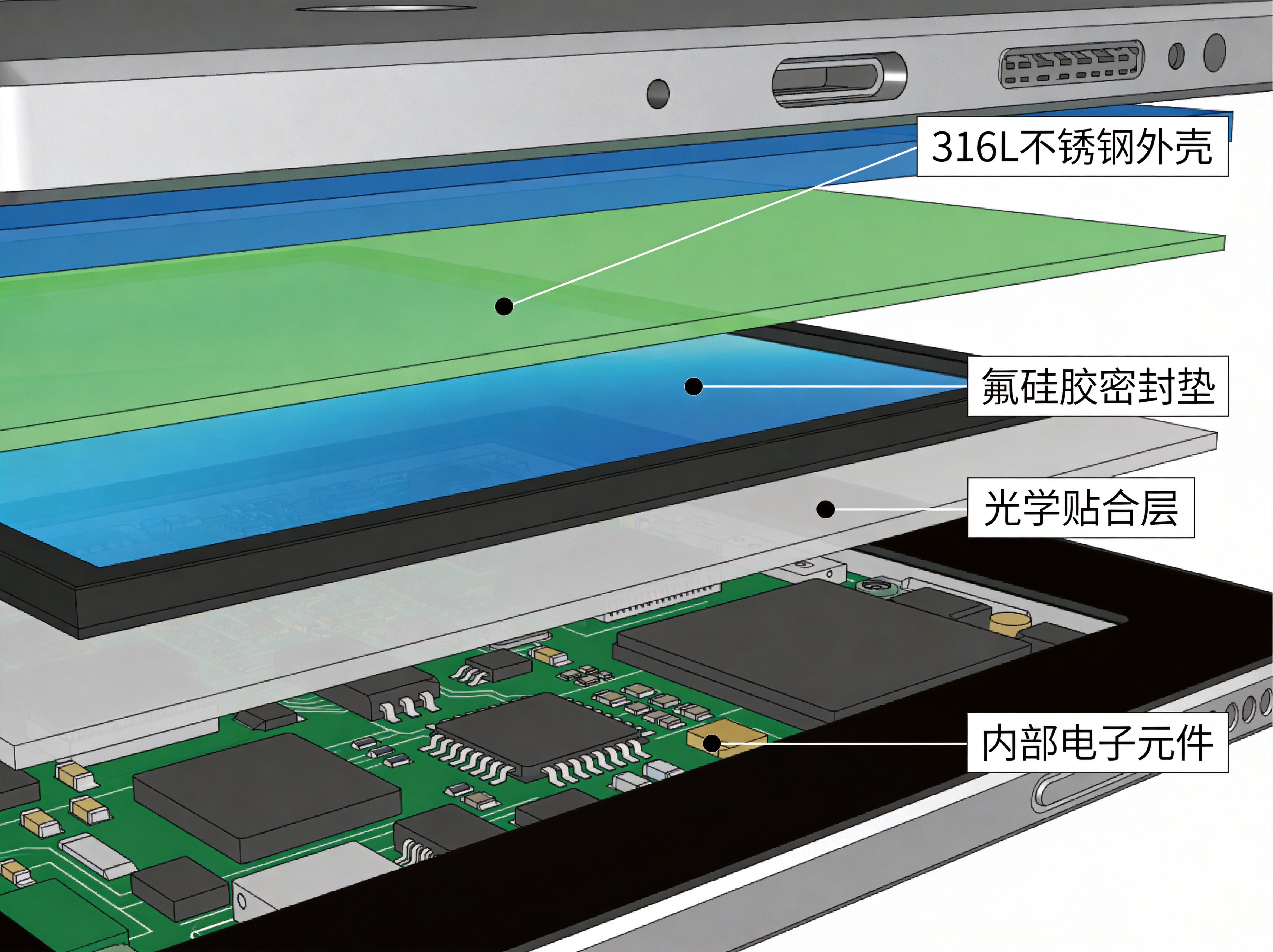
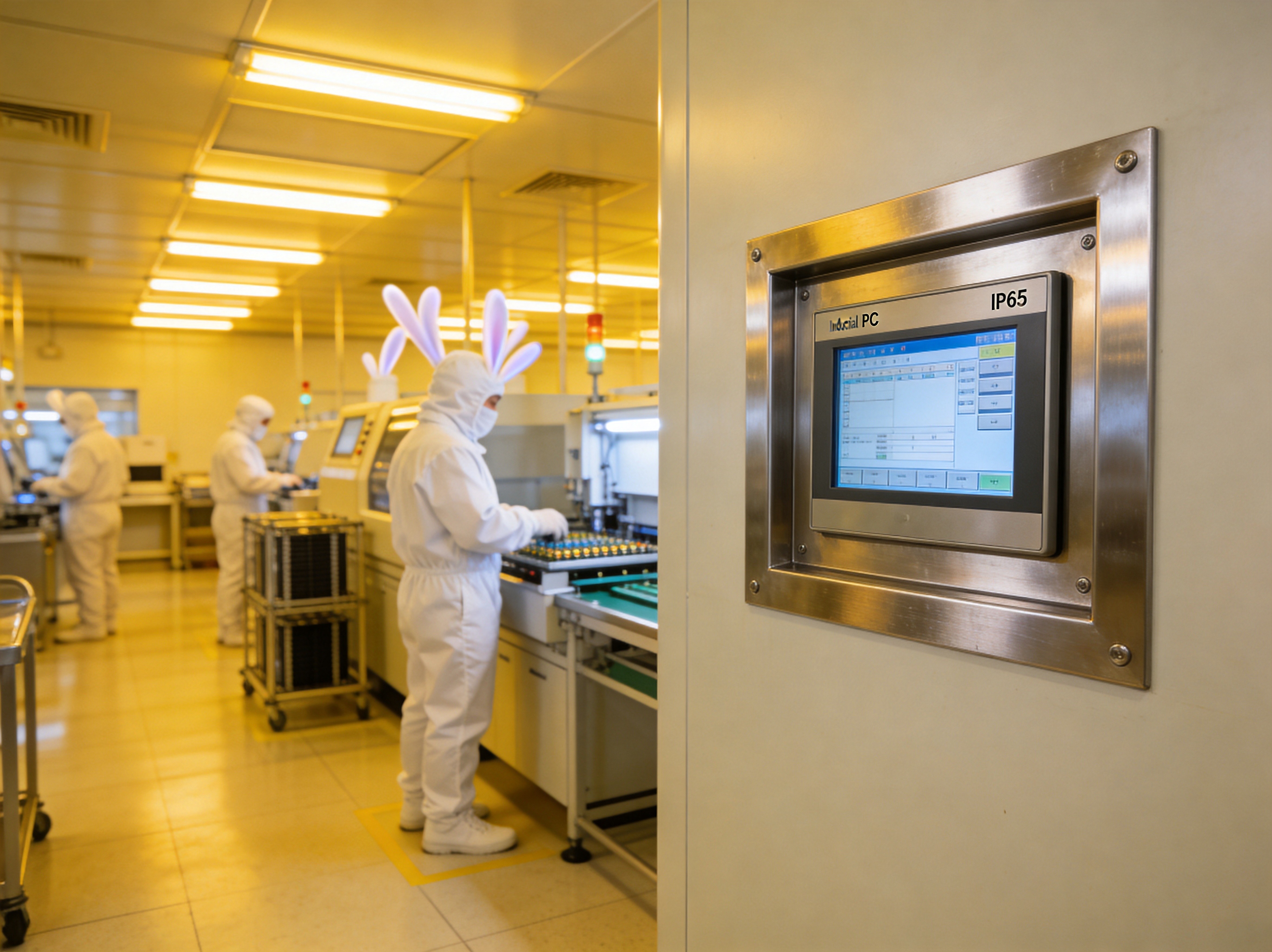
Cleanroom computing starts with the enclosure. Semiconductor fabs typically operate at ISO Class 5 or better, meaning no more than 3,520 particles of 0.5 micron or larger per cubic meter of air. A standard industrial panel PC with a cooling fan would fail this requirement instantly, circulating particulates and disrupting laminar airflow patterns. The solution is a fully sealed, fanless design with a stainless steel or electropolished aluminum enclosure that resists outgassing and withstands aggressive cleaning protocols including hydrogen peroxide vapor and isopropyl alcohol wipes. The touchscreen surface must be optically bonded to eliminate crevices where contaminants could accumulate. Every cable gland, connector port, and mounting bracket must preserve the cleanroom’s pressure cascade. KOXIAN has developed a cleanroom panel PC series meeting these requirements through a seam-welded 316L stainless steel chassis, IP65-rated front bezel, and passive thermal management that dissipates heat through the enclosure surface rather than moving air.
Wafer Fab Deployment: Process Control and Defect Monitoring
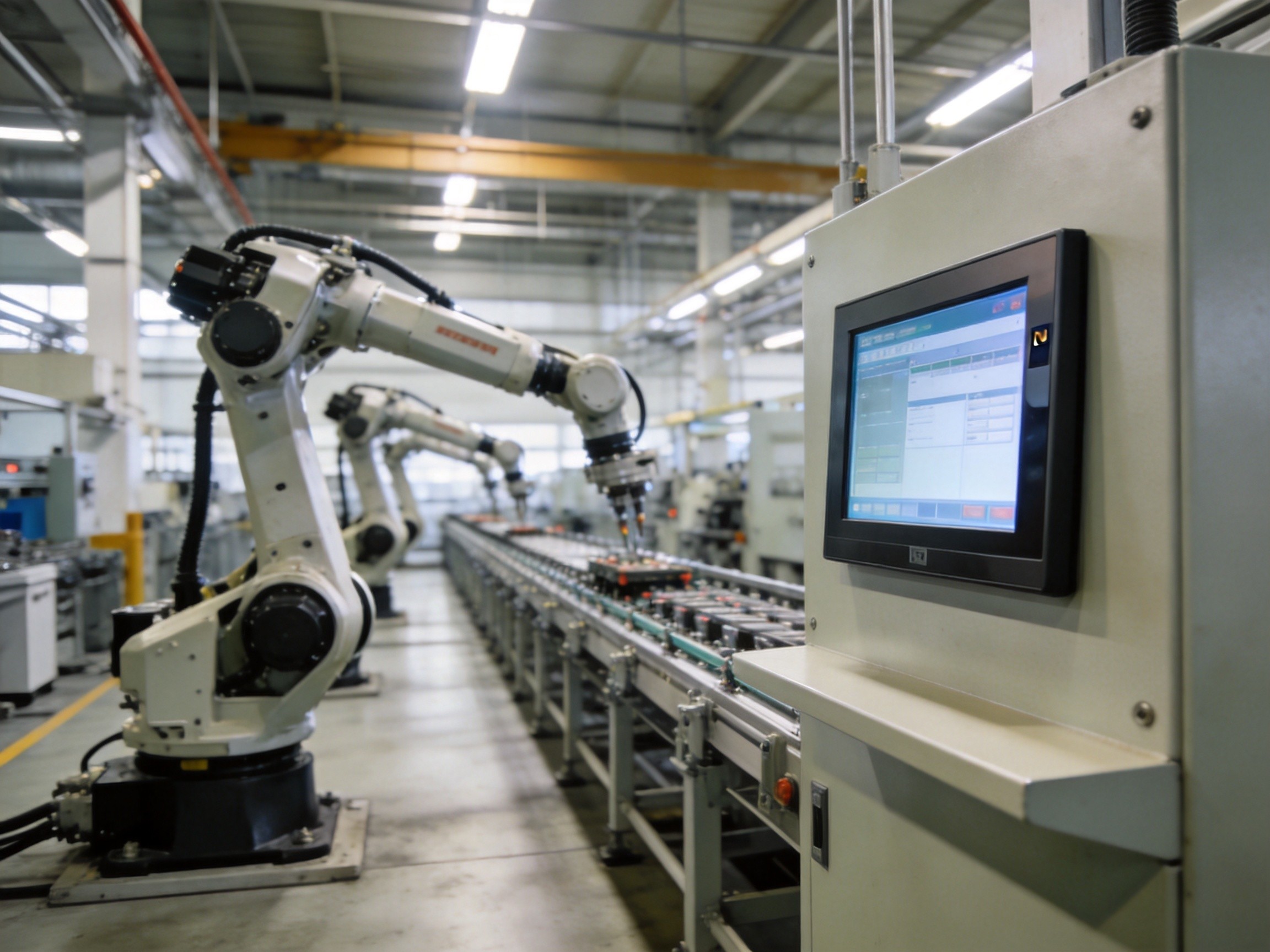
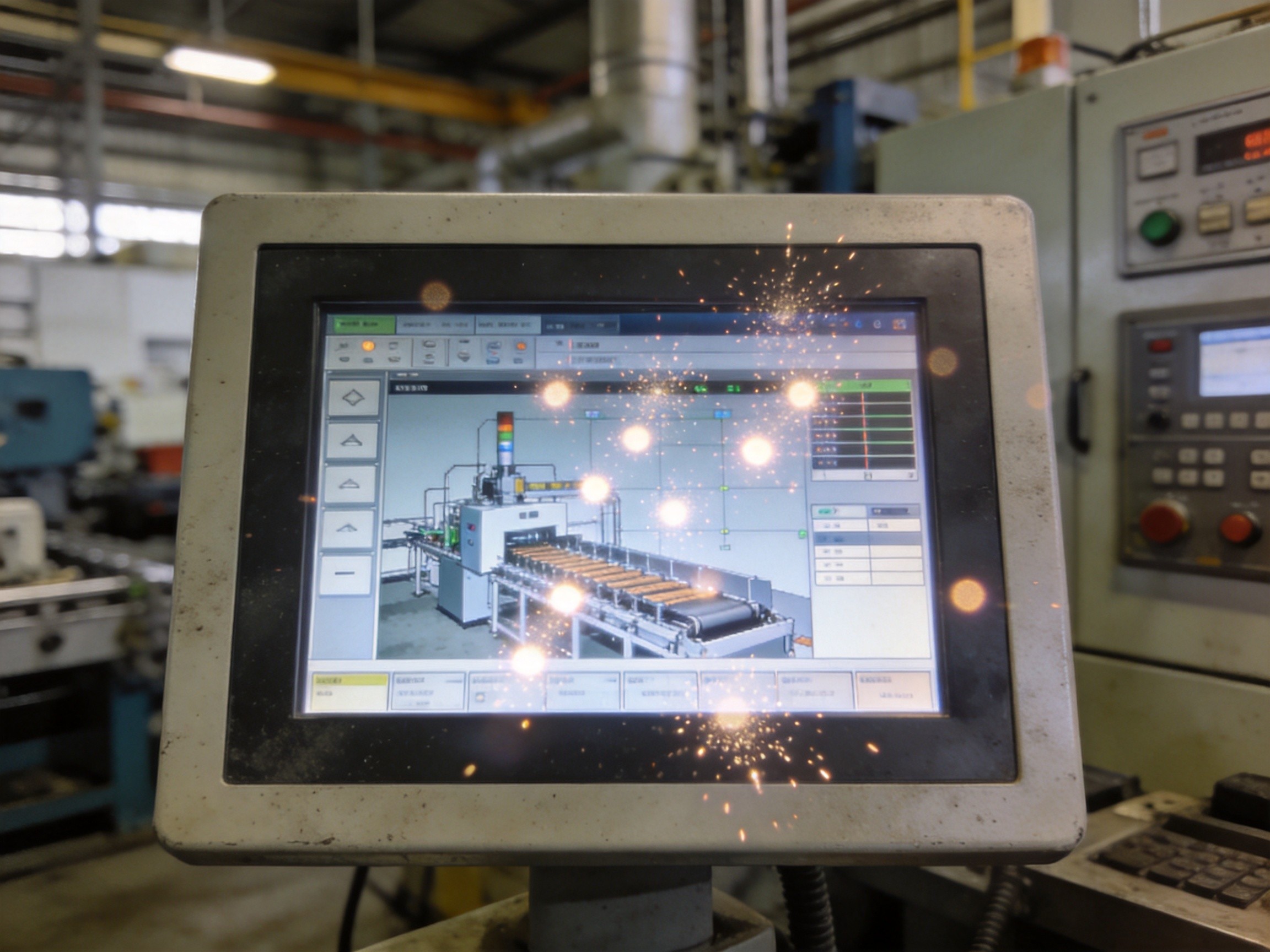
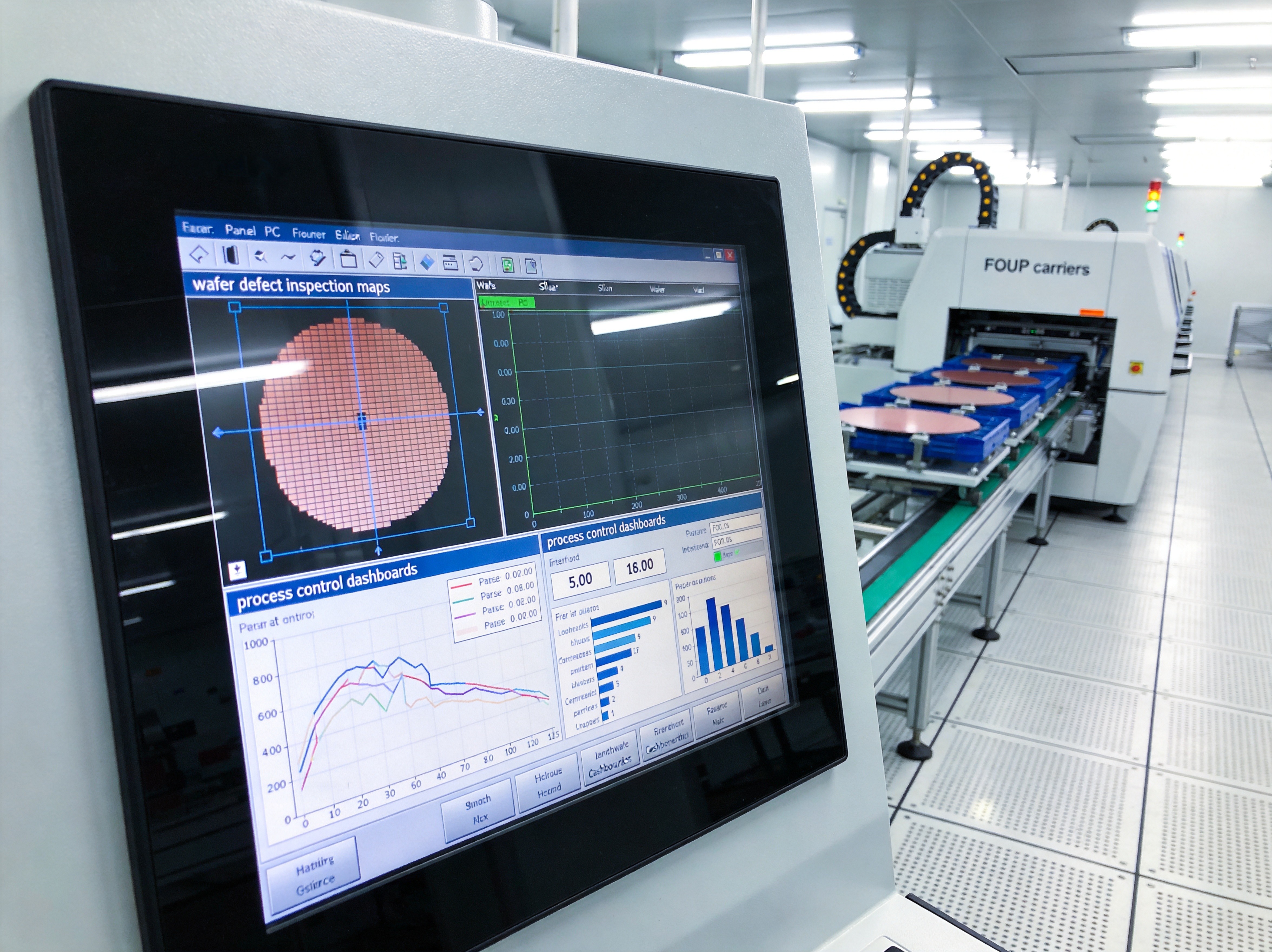
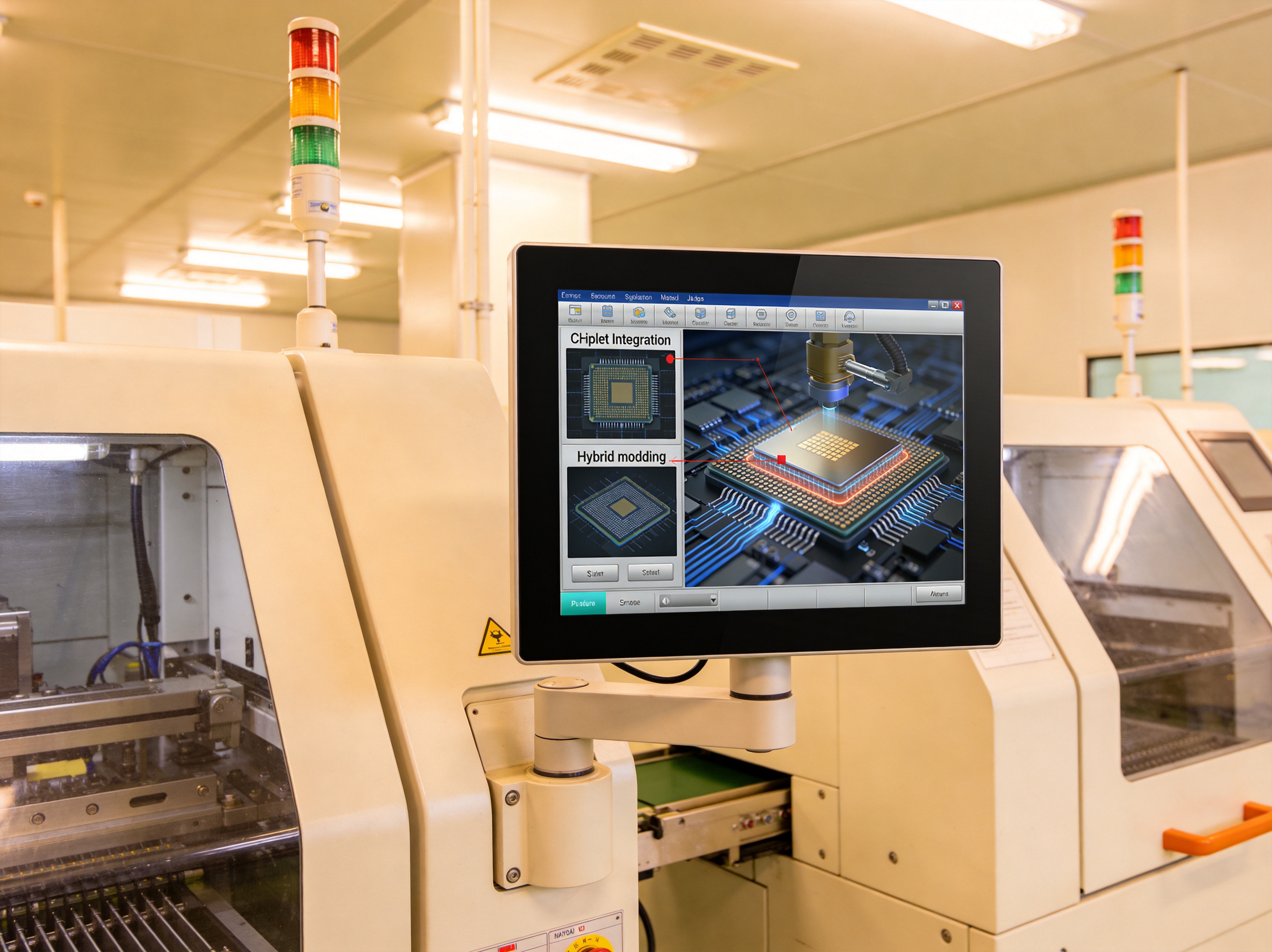
In a working fab, panel PCs serve as the operator interface for nearly every process step. Lithography tracks, etch chambers, deposition tools, and metrology stations all require local computing nodes that display real-time process data, accept operator input, and log every interaction for traceability. The SEMICON Taiwan 2026 conference, held July 15 in Taipei, dedicated significant floor space to smart manufacturing solutions that connect individual tool interfaces into a unified fab-wide data fabric. The trend toward advanced packaging—chiplet integration, hybrid bonding, and 3D stacking—adds further complexity, requiring panel PCs that handle high-resolution imaging data from multiple inspection sources simultaneously. The projected 300-millimeter fab equipment spending crossing the 150-billion-dollar threshold in 2027 reflects not just capacity expansion but a qualitative upgrade in process control infrastructure, where edge computing at the tool level is becoming a competitive differentiator for fab operators.
Advanced Packaging Environments: Precision and Throughput
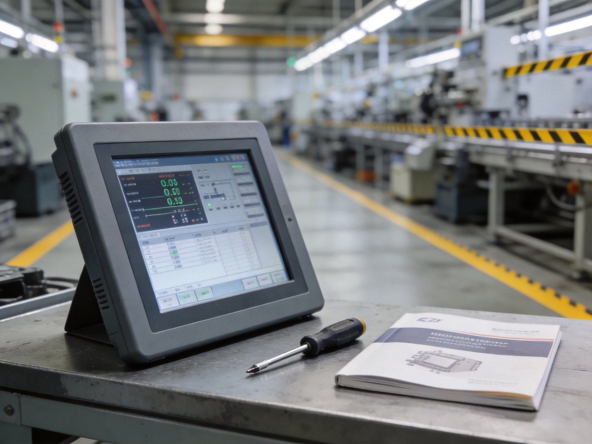
Advanced packaging represents the fastest-growing segment of semiconductor manufacturing, and it places unique demands on operator interface hardware. Unlike front-end wafer processing where individual tools operate in relative isolation, advanced packaging lines are highly integrated, with multiple process modules connected by automated material handling. Panel PCs in these environments must communicate across a distributed control architecture while maintaining sub-second response times for operator interventions. The visual requirements are also more demanding: operators need to inspect micro-bump arrays, through-silicon via alignment, and interposer quality at magnification levels requiring high-resolution displays with excellent color accuracy. KOXIAN panel PCs deployed in these environments feature optically bonded 4K displays with anti-glare coatings that maintain visibility under the bright yellow lighting used in photolithography-adjacent areas, ensuring operators can identify sub-micron defects without eye strain.
Data Integrity and Traceability in Fab Environments
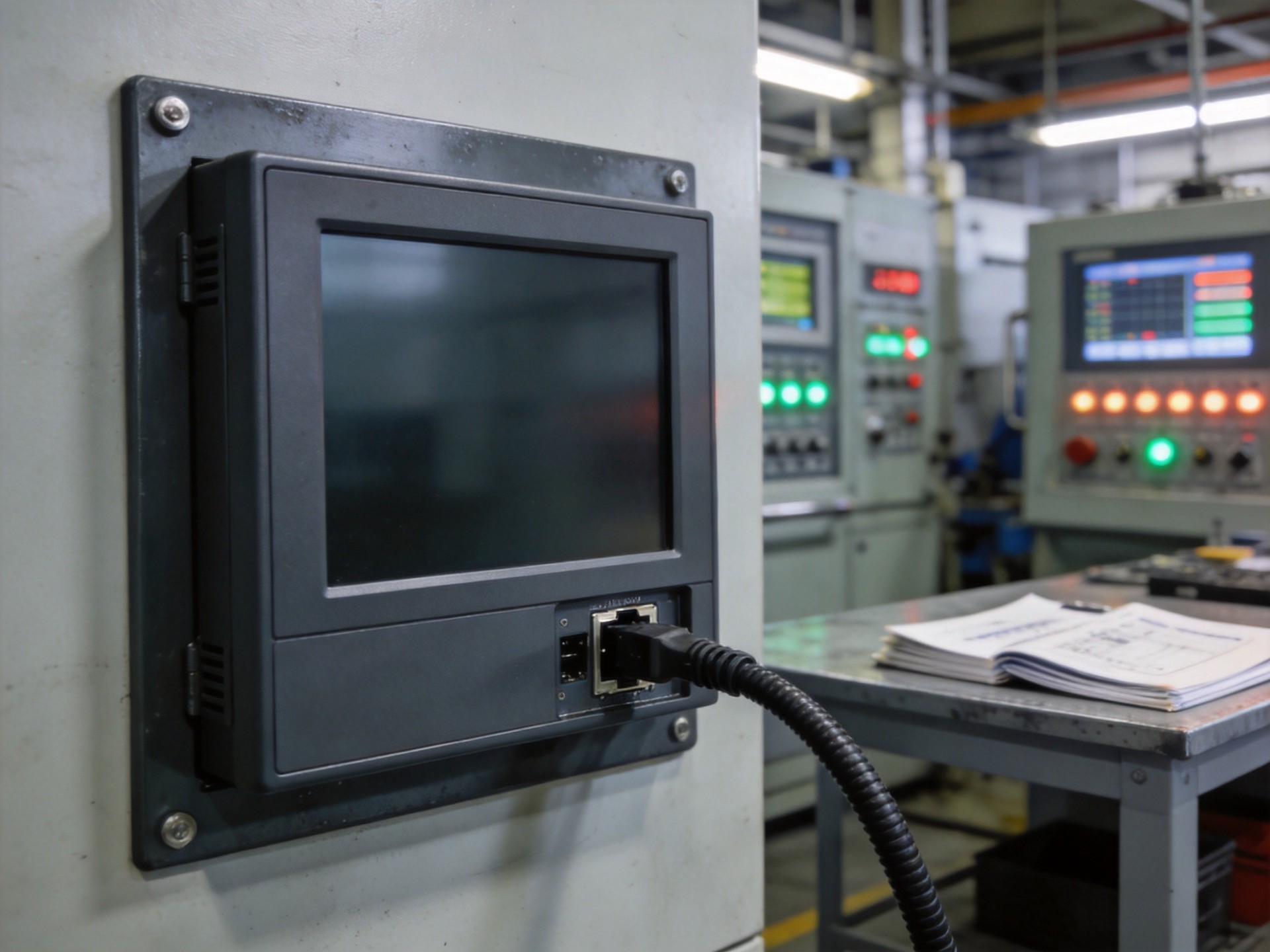
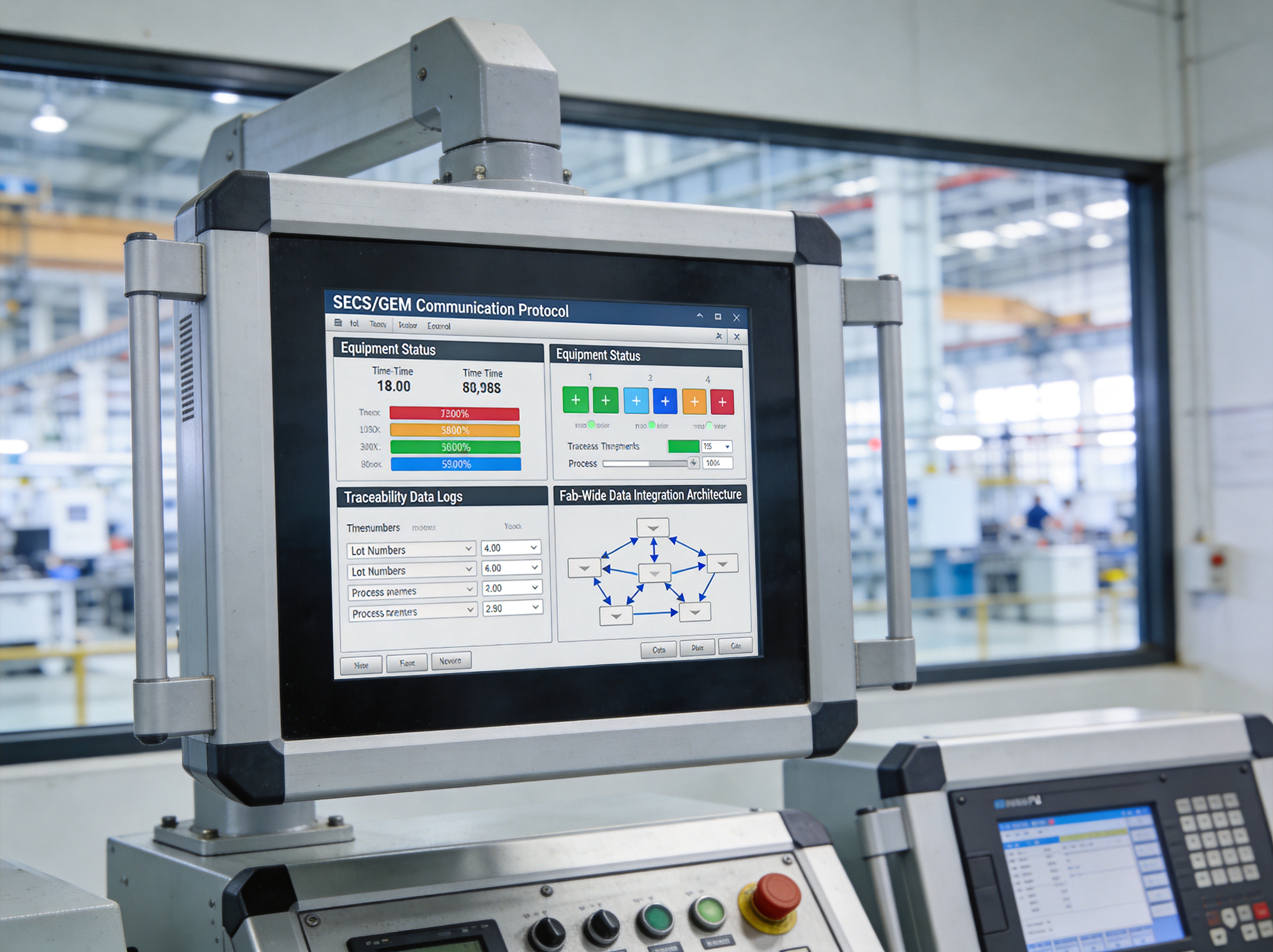
Semiconductor manufacturing operates under strict traceability mandates. Every wafer, every lot, every process recipe modification must be logged with timestamps, operator identification, and equipment status. Panel PCs at the tool interface are the primary data entry and verification point for this chain of custody. They must support industry-standard fab communication protocols while maintaining local data buffering that preserves records even during network interruptions. The computing hardware must also be validated against the fab’s change management procedures, which can require months of qualification testing before a new panel PC model is approved for production deployment. For fab operators investing in the equipment expansion that will drive spending past 150 billion dollars in 2027, the reliability and traceability features of their operator interface hardware are not optional—they are core to maintaining yield, compliance, and audit readiness across every process step.
As semiconductor manufacturing pushes toward smaller nodes and more complex packaging architectures, the computing hardware that supports fab operations must evolve in parallel. The panel PCs deployed on the cleanroom floor today process more data, support higher-resolution displays, and maintain stricter contamination controls than the server-class hardware of a decade ago. With fab equipment investment accelerating and smart manufacturing initiatives transforming how semiconductors are produced, the role of industrial-grade, cleanroom-qualified computing at the tool interface will only grow in importance. The silicon that powers the world’s most advanced chips deserves equally advanced operator interface hardware.