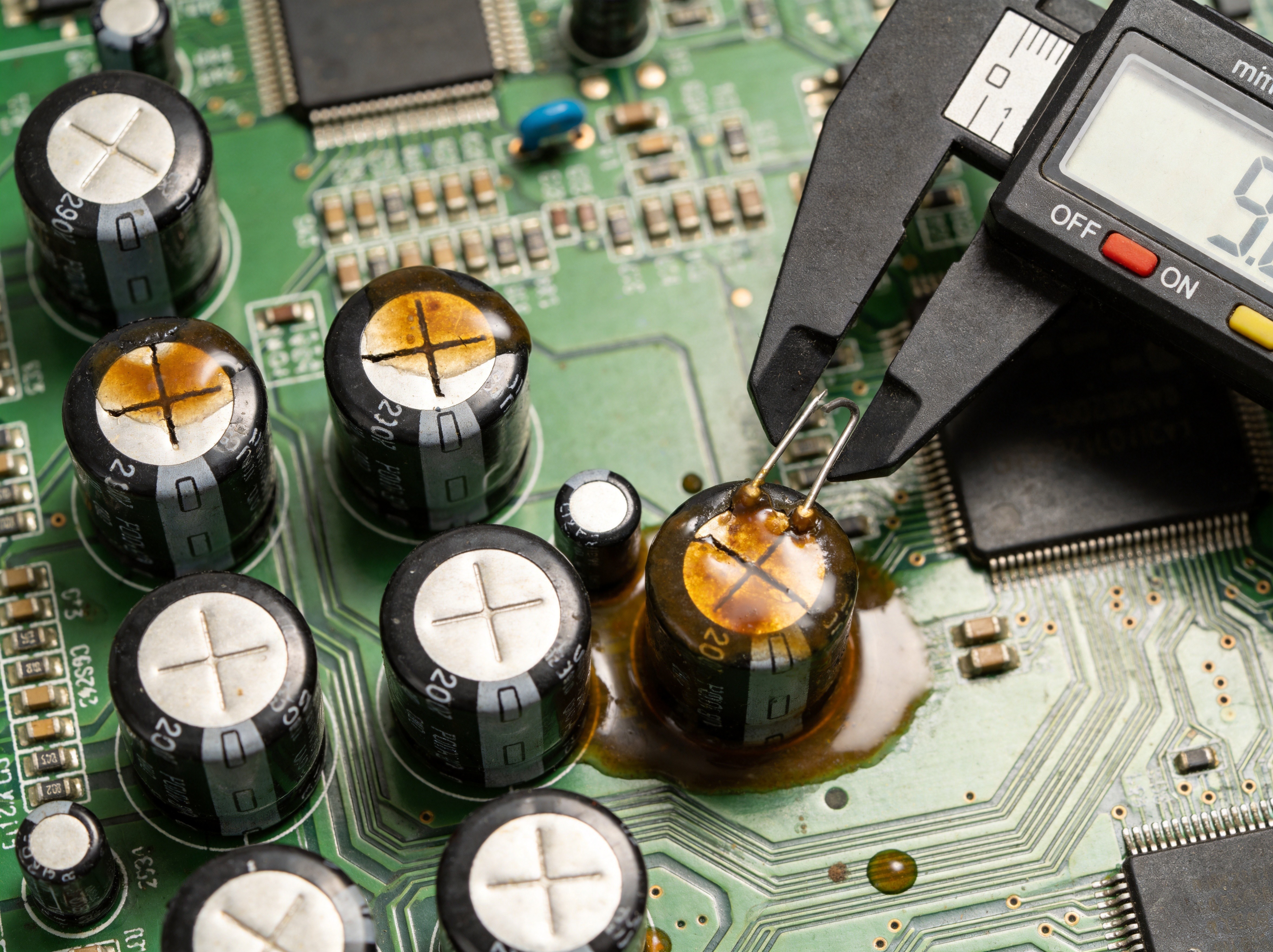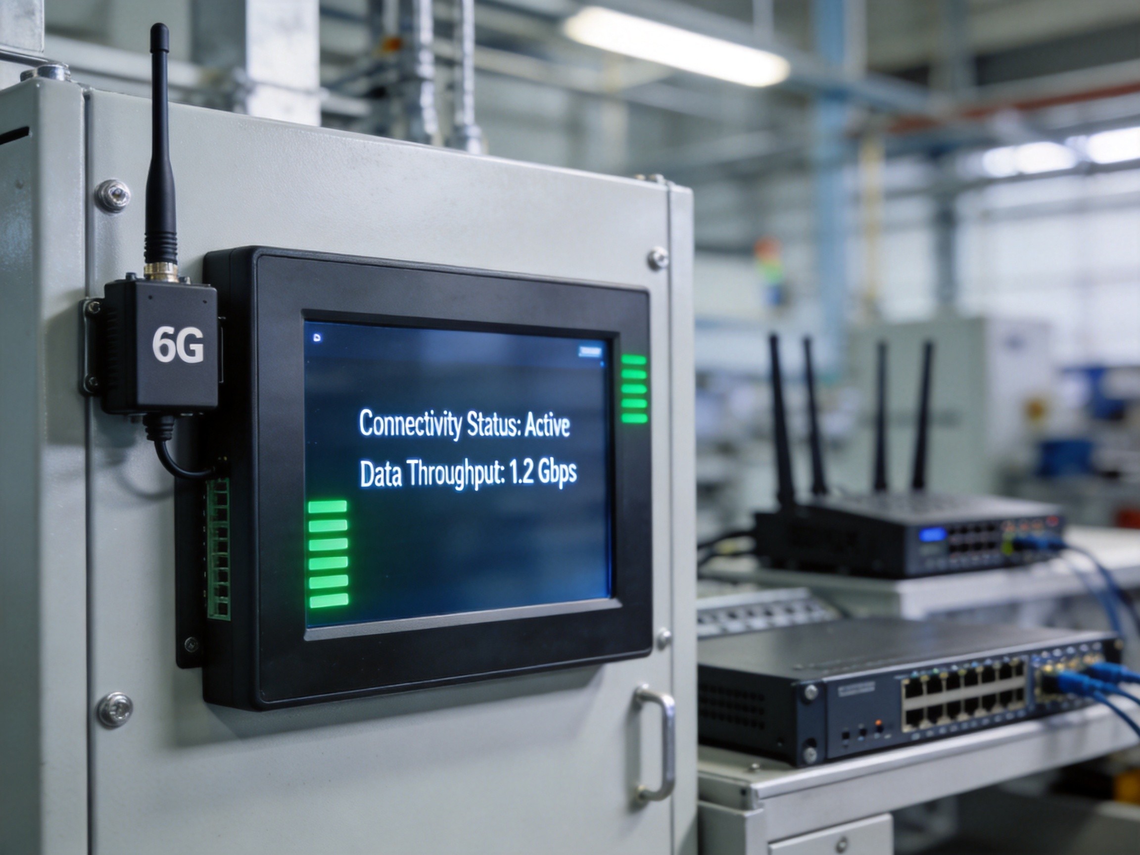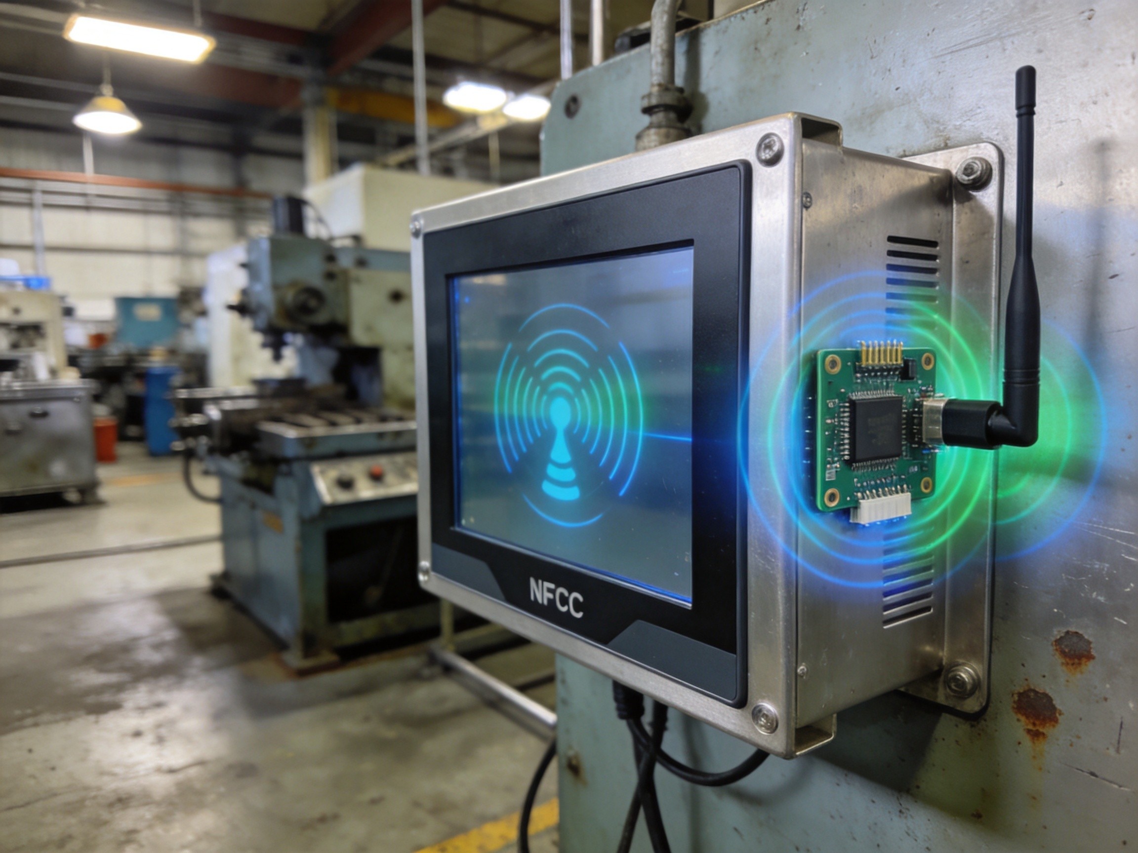
Photovoltaic inverters convert DC from solar arrays into grid-synchronized AC using high-frequency switching topologies operating at 20 kHz to over 100 kHz. That switching action is also the source of a persistent and often underestimated problem. Every rapid voltage transition generates broadband EMI that radiates through the air and conducts along power and signal cables. When an industrial panel PC data acquisition terminal is installed in the same substation, its sensitive analog front-end sits directly in the EMI crossfire. The result: corrupted sensor readings, intermittent dropouts, and in severe cases, permanent hardware damage. With mandatory inverter efficiency standards requiring continuous monitoring, the EMI problem has moved from inconvenience to compliance risk.

Conducted EMI: The Silent Data Corrupter
Conducted EMI travels along the cables connecting the data acquisition terminal to its sensors. When a PV inverter switches its IGBT or SiC MOSFET power devices, the rapid voltage slew rate—often exceeding 50 kV/µs—induces high-frequency common-mode currents that flow through the ground plane and into DC power supply lines shared by the monitoring equipment. These currents manifest as voltage spikes on analog sensor signals. A thermocouple may see a 50 mV EMI spike riding on a 10 mV signal, destroying measurement accuracy. Current transformers fare worse because their secondary windings act as antennas for the magnetic field component. The terminal’s analog-to-digital converter cannot distinguish between the real signal and the EMI artifact, producing data that looks plausible but is technically wrong.
Radiated EMI: The Airborne Threat
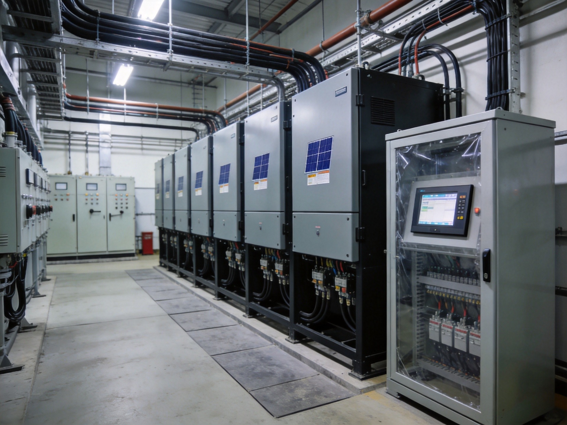
Radiated EMI does not need a physical connection. High-frequency switching currents in the inverter’s power stage create magnetic fields that couple into nearby cables and PCB traces through the air. The DC bus—a long, unshielded conductor carrying hundreds of amps with high di/dt—acts as an unintentional transmitting antenna. The terminal’s touchscreen controller, Ethernet PHY, and USB interfaces are particularly vulnerable because their signal levels are low relative to the EMI wavelength. Engineers have observed radiated EMI from a 500 kW central inverter causing the capacitive touchscreen on a co-located panel PC to register phantom touches, making the interface unusable. In another documented case, radiated interference induced sufficient common-mode voltage on an unshielded Ethernet cable to corrupt TCP checksums, causing repeated network disconnections during peak inverter output hours.
Protection Strategies: A Three-Layer Defense
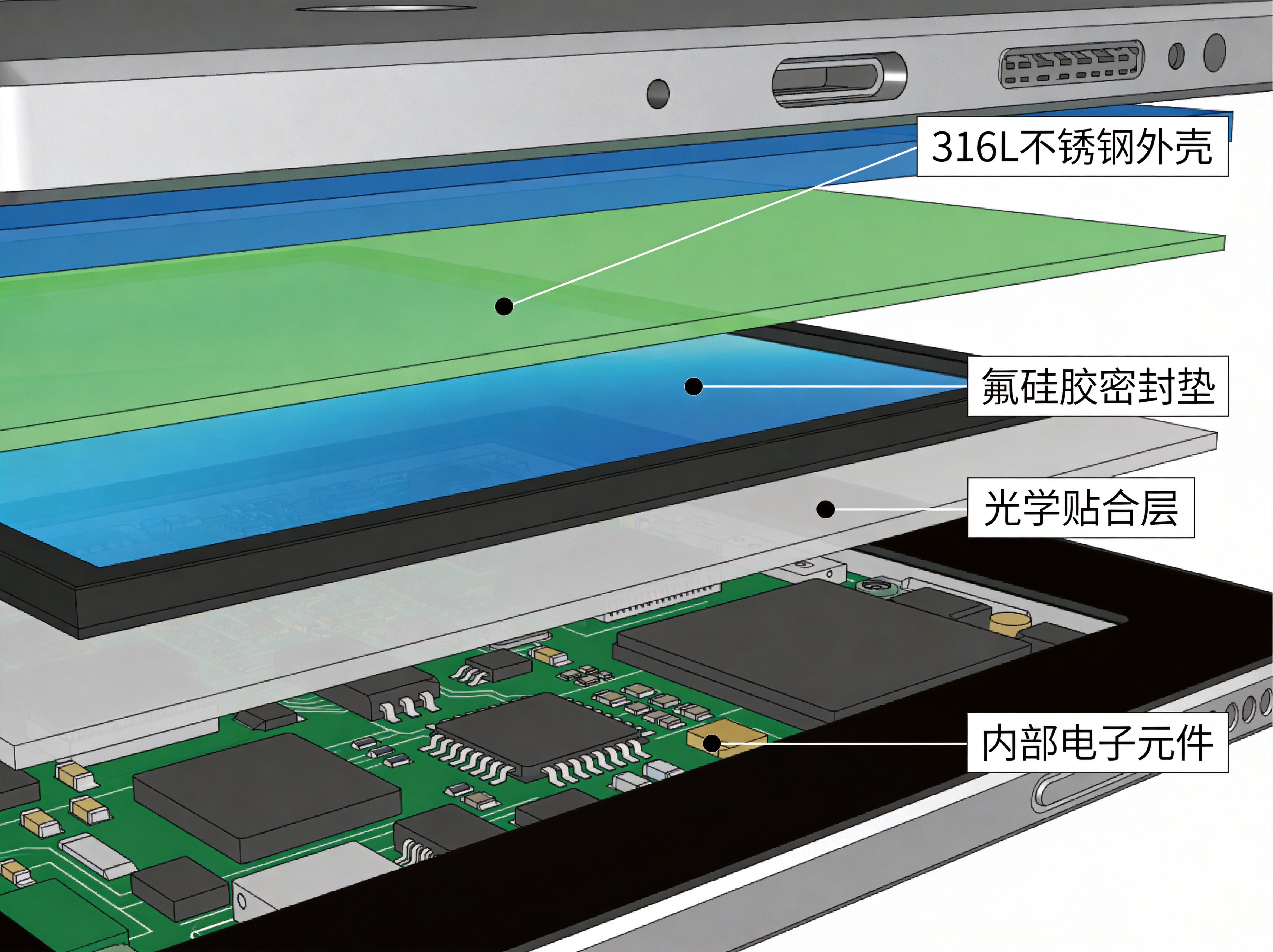
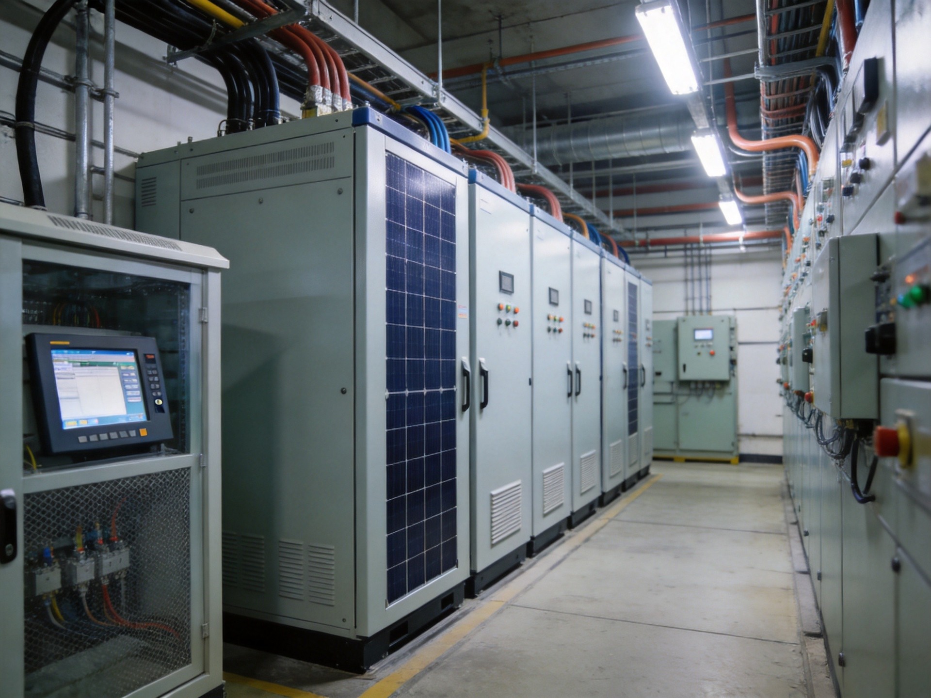
Effective EMI protection follows a three-layer defense-in-depth approach. Layer one: physical separation and shielding—the industrial panel PC should be installed in a grounded metallic enclosure, minimum two meters from the nearest inverter power stage, with shielded connectors and 360-degree bonding at all cable entry points. Layer two: signal conditioning—each analog input channel protected by a differential amplifier with high common-mode rejection ratio, followed by a low-pass filter with cutoff below the inverter switching frequency, plus ferrite beads on digital I/O lines. Layer three: power isolation—the terminal powered through an isolated DC-DC converter providing at least 1,500 V of galvanic isolation. Industrial panel PCs engineered with these protection measures at the board level—including fully enclosed aluminum chassis that act as Faraday cages—provide a pre-validated path to EMI immunity.
Validation: Beyond the Datasheet
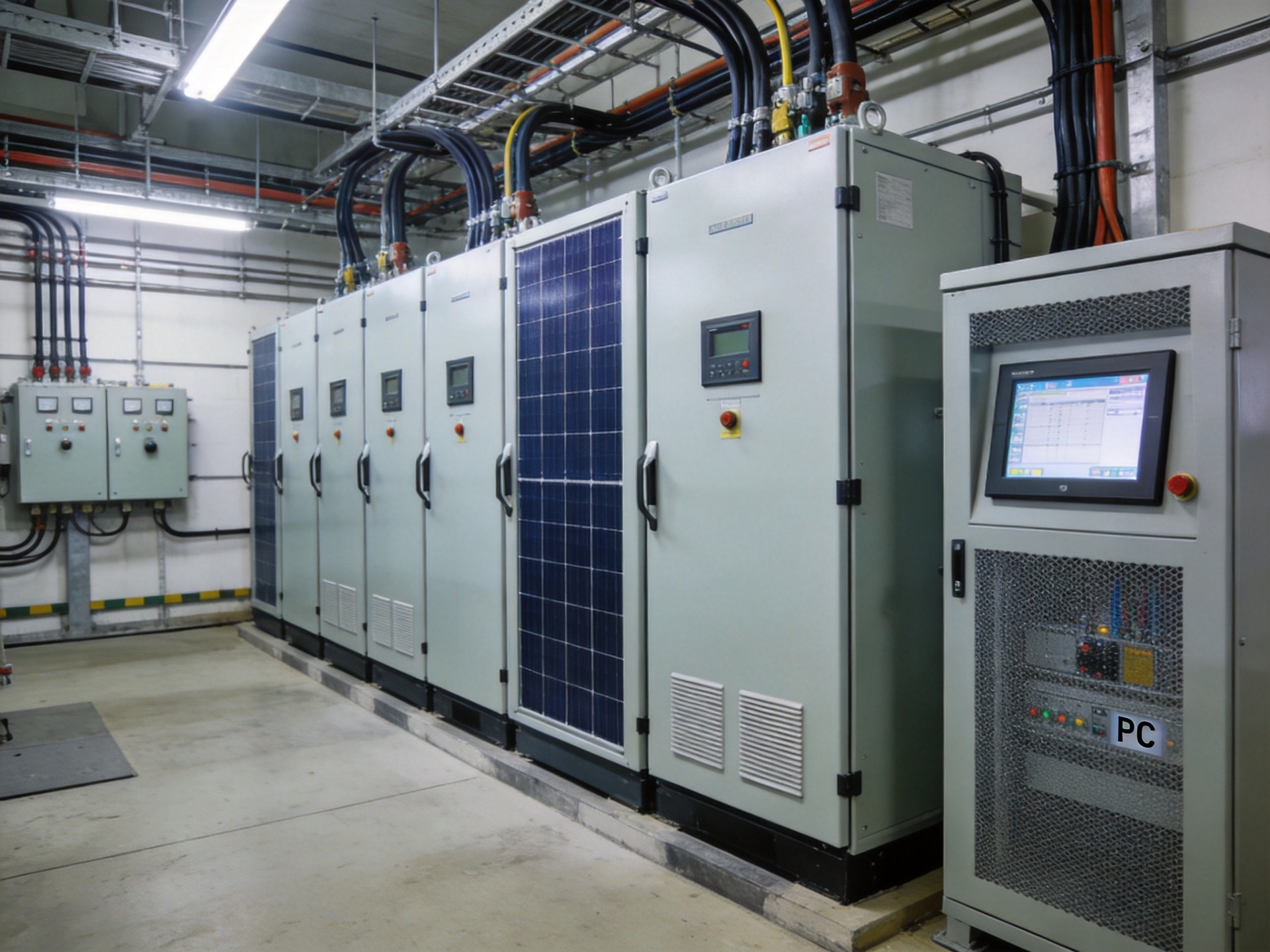
A datasheet claiming IEC 61000-4 compliance is a starting point, not a guarantee. The standard’s test levels—10 V/m for radiated immunity, 2 kV for conducted immunity on power lines—may not reflect the actual EMI environment inside a substation with multiple 500 kW inverters switching simultaneously. Field validation should include a site survey with a spectrum analyzer from 150 kHz to 80 MHz for conducted and 30 MHz to 1 GHz for radiated emissions. The terminal should be tested in situ at full inverter load, comparing readings against a battery-powered reference instrument in a shielded location. Hardware platforms that have undergone extended field validation in high-EMI environments, such as those deployed by manufacturers with deep experience in power electronics integration, offer confidence that laboratory testing alone cannot provide. As efficiency standards drive higher switching frequencies and faster edge rates, robust terminal hardening becomes a prerequisite, not an afterthought.
PV inverter EMI cannot be solved with a single ferrite clamp or a software filter. It requires a systematic approach to shielding, signal conditioning, and power isolation, implemented at the hardware architecture level. For operators facing the dual mandate of maximizing inverter efficiency and maintaining continuous compliance monitoring, the data acquisition terminal must be selected with the same rigor as the power electronics it monitors.