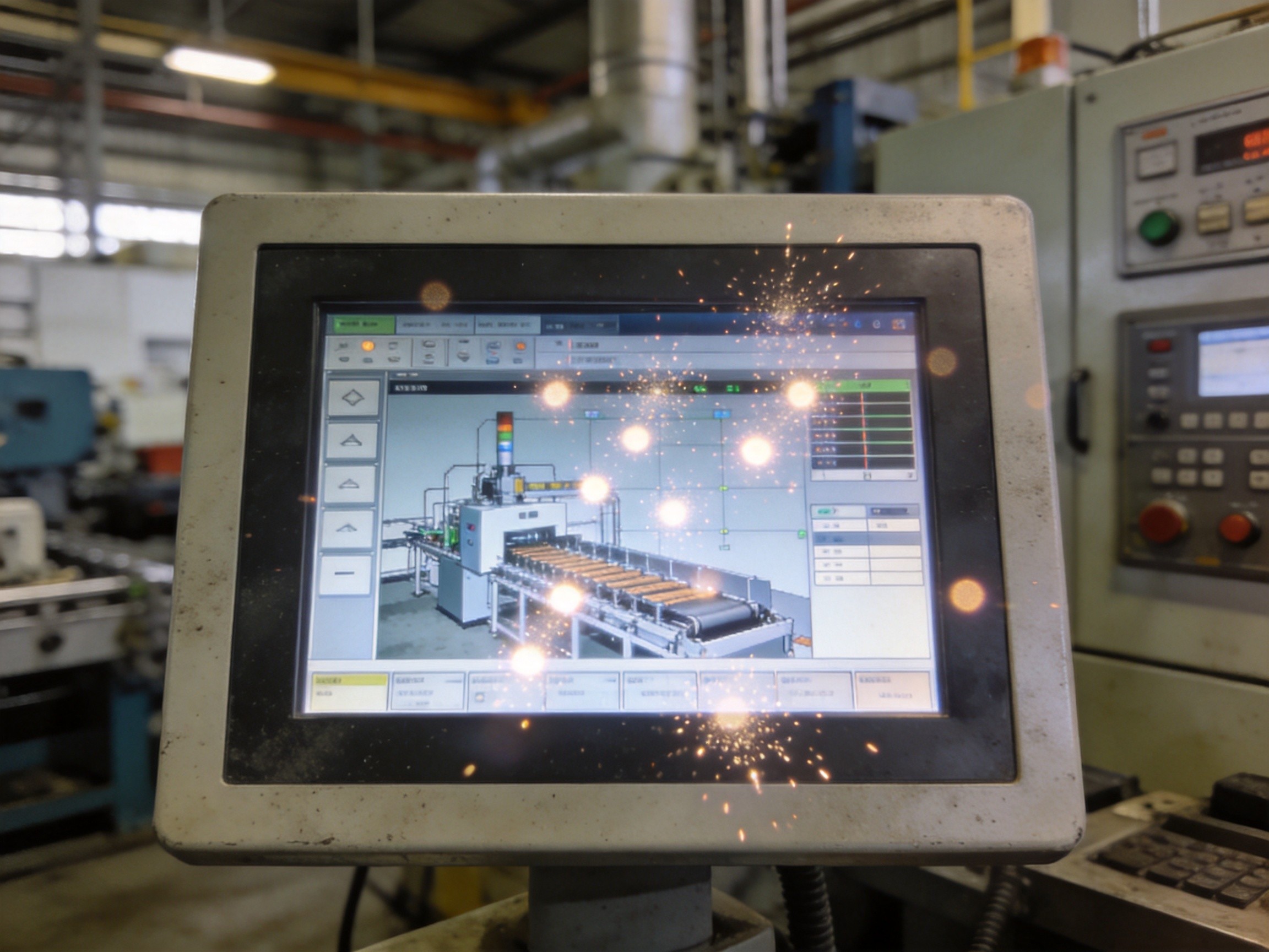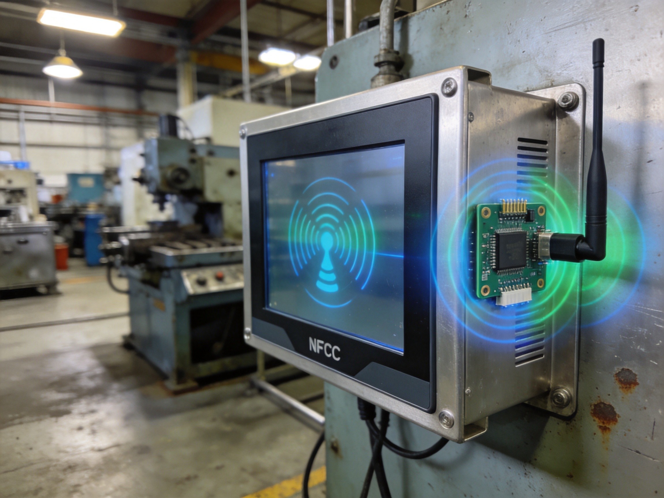
The semiconductor industry is undergoing a dramatic architectural shift, and the implications for industrial edge computing are only beginning to be understood. In July 2026, TSMC disclosed that its 2-nanometer process node—the first to adopt gate-all-around nanosheet transistors—had accumulated four times the tape-outs of its 3nm predecessor at the same stage, contributing 3% of wafer revenue in just its second quarter of production. Simultaneously, TSMC CEO C.C. Wei flagged a resurgence in CPU demand driven by agentic AI workloads, reshaping how data centers allocate silicon. But while the cloud computing world races toward 2nm accelerators and rack-scale GPU deployments, the industrial edge operates under entirely different constraints—and demands a fundamentally different silicon strategy.
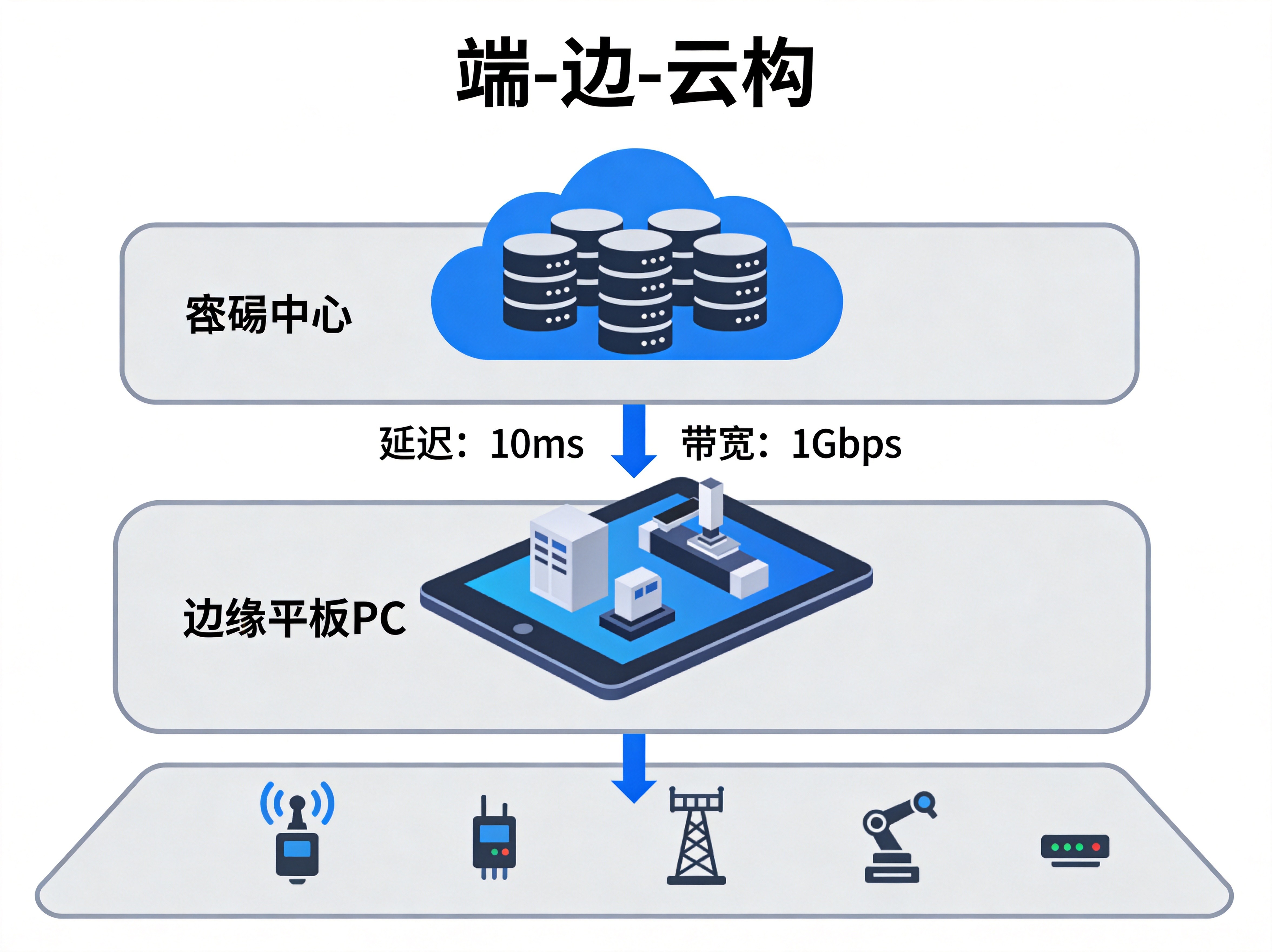
The Cloud Is Racing to 2nm—But the Edge Cannot Follow
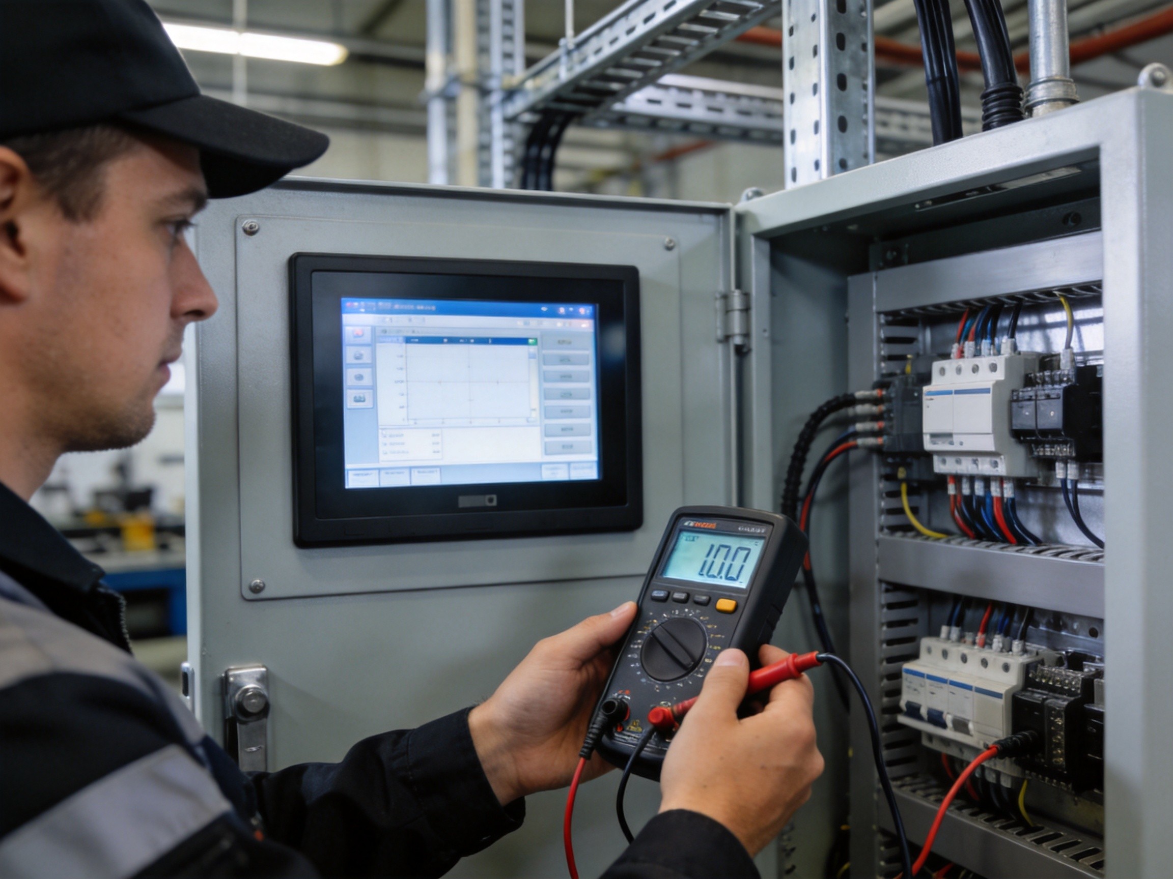
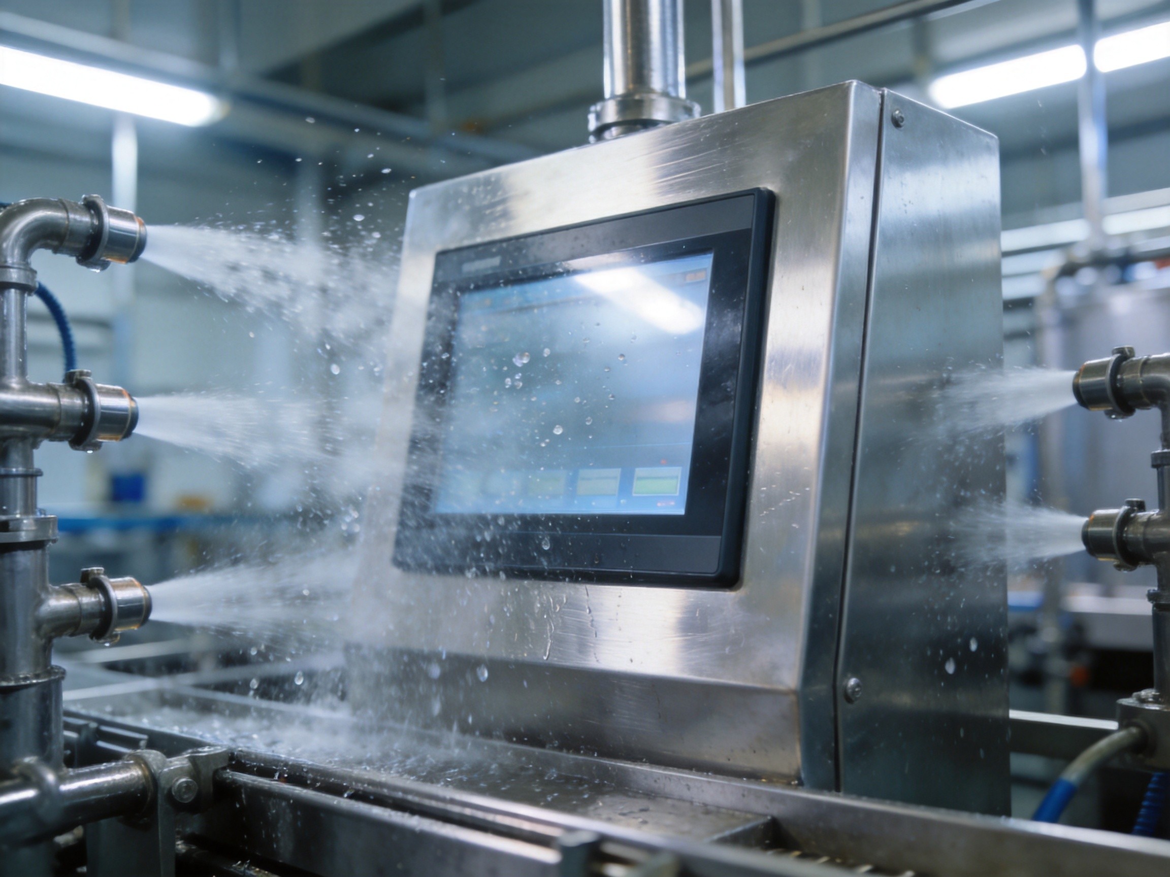
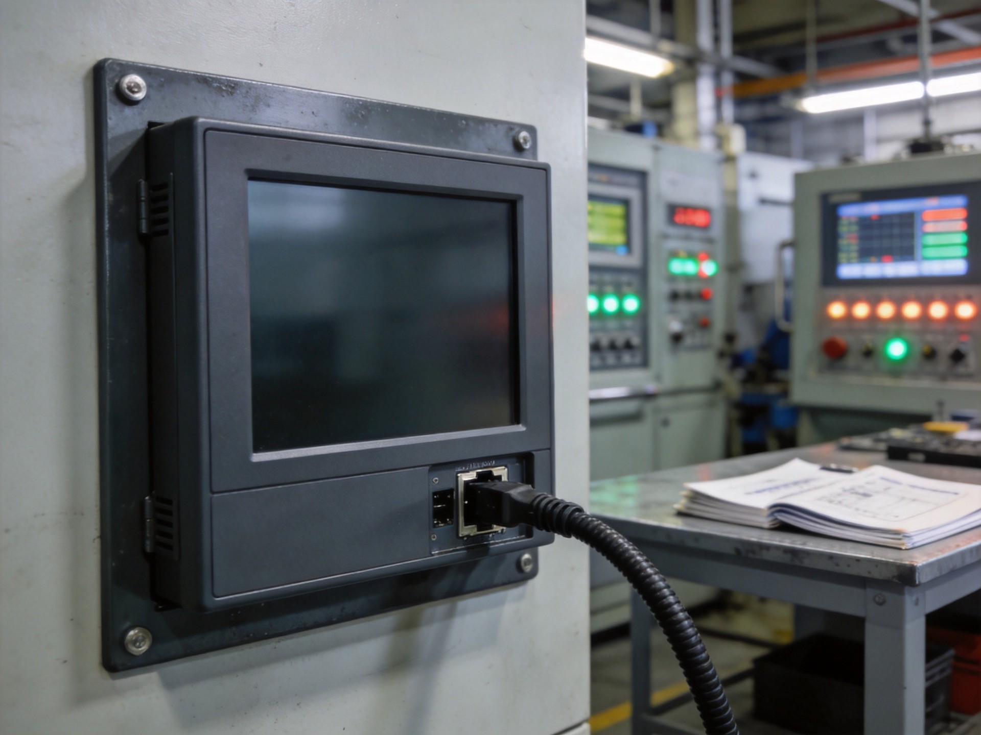
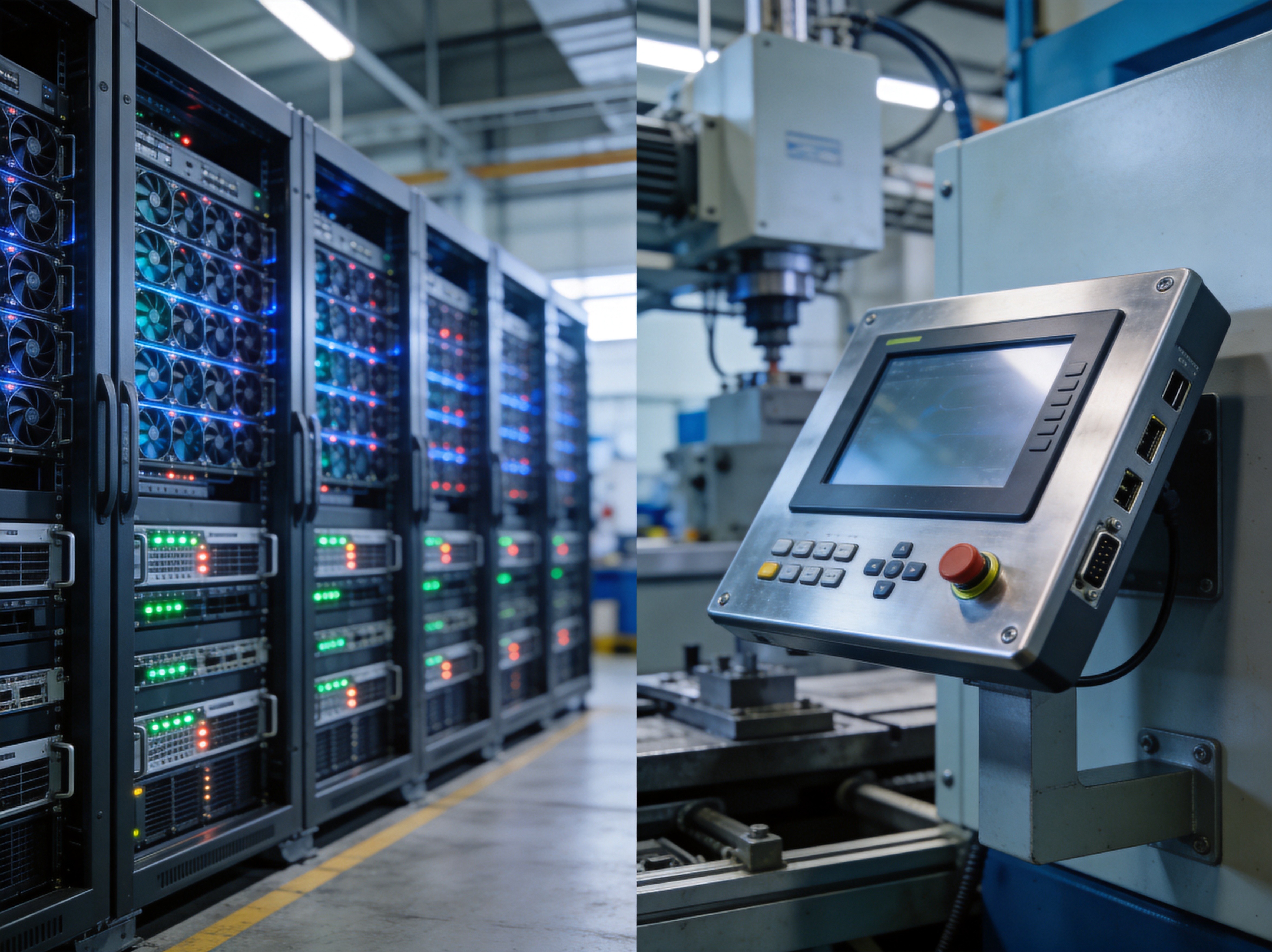
TSMC’s 2nm node, designated N2, entered volume production in Q4 2025 and has already achieved 90% yield, with monthly output ramping toward 140,000 wafers by year-end. The performance gains are substantial: 10 to 15 percent higher speed at the same power, or 25 to 30 percent lower power at the same speed, versus the 3nm N3E node. Google, Apple, Qualcomm, and NVIDIA are all lining up for capacity. Yet none of this directly benefits the industrial edge. The reason is simple: cutting-edge nodes optimize for transistor density and peak compute throughput, but edge deployments in factories, water treatment plants, and outdoor installations prioritize thermal envelope, long-term supply stability, and tolerance for wide operating temperature ranges. A 2nm chip designed for a liquid-cooled data center rack offers no advantage when the target environment is a panel PC mounted inside a chemical dosing station operating at 55 degrees Celsius ambient.
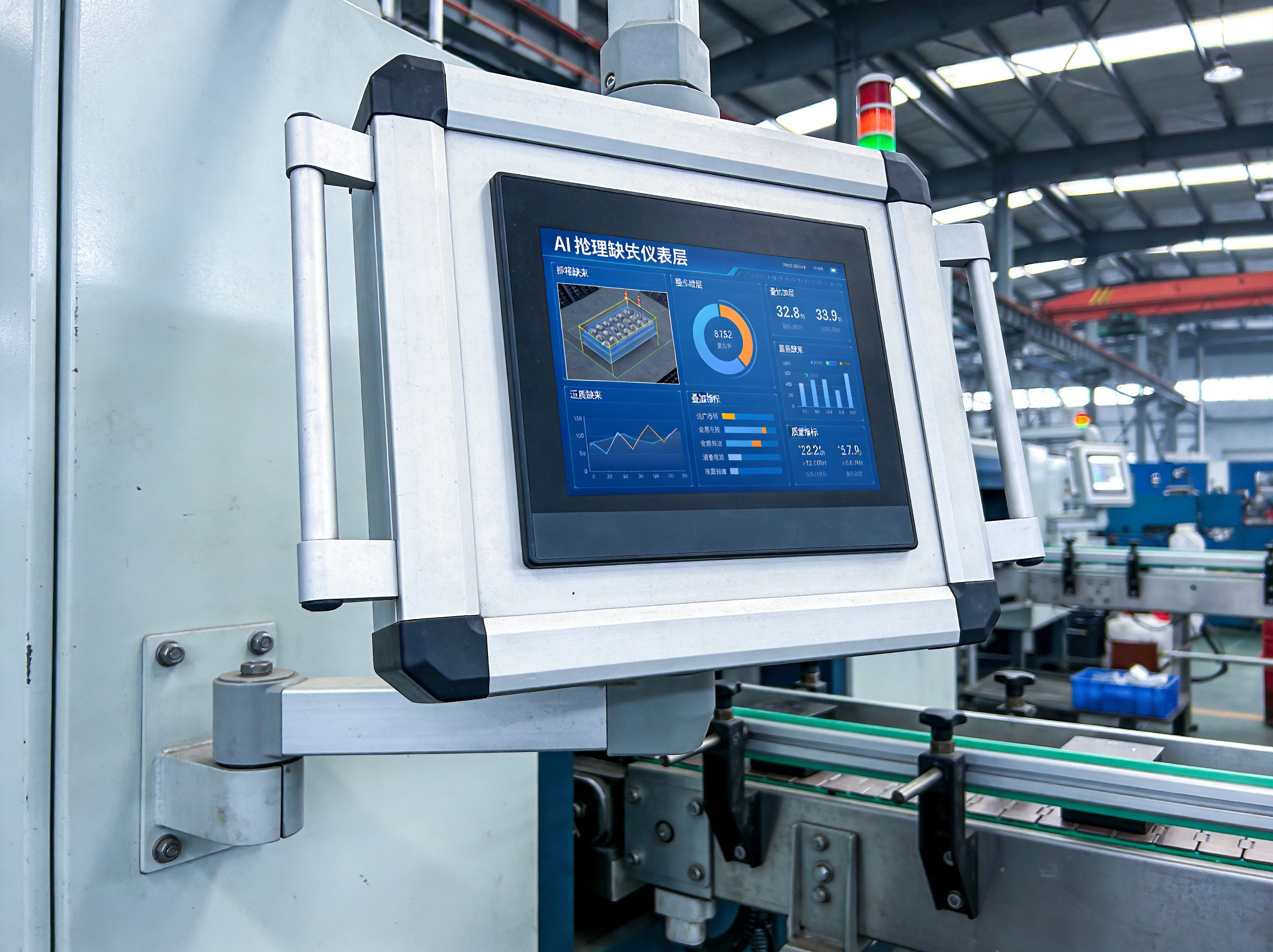
Agentic AI Is Reshaping CPU Demand—In Both Directions
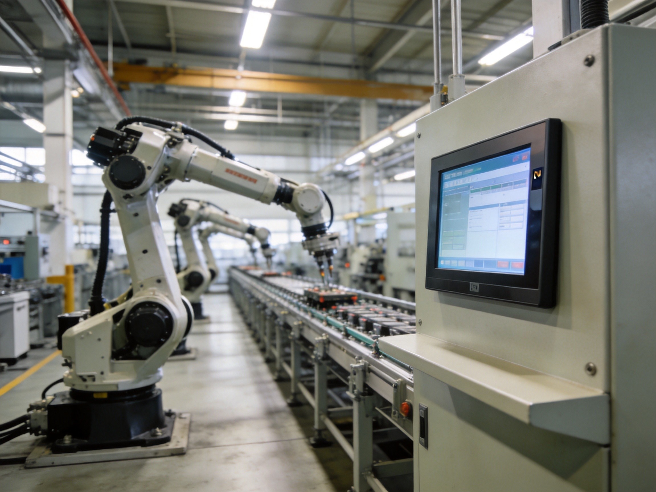
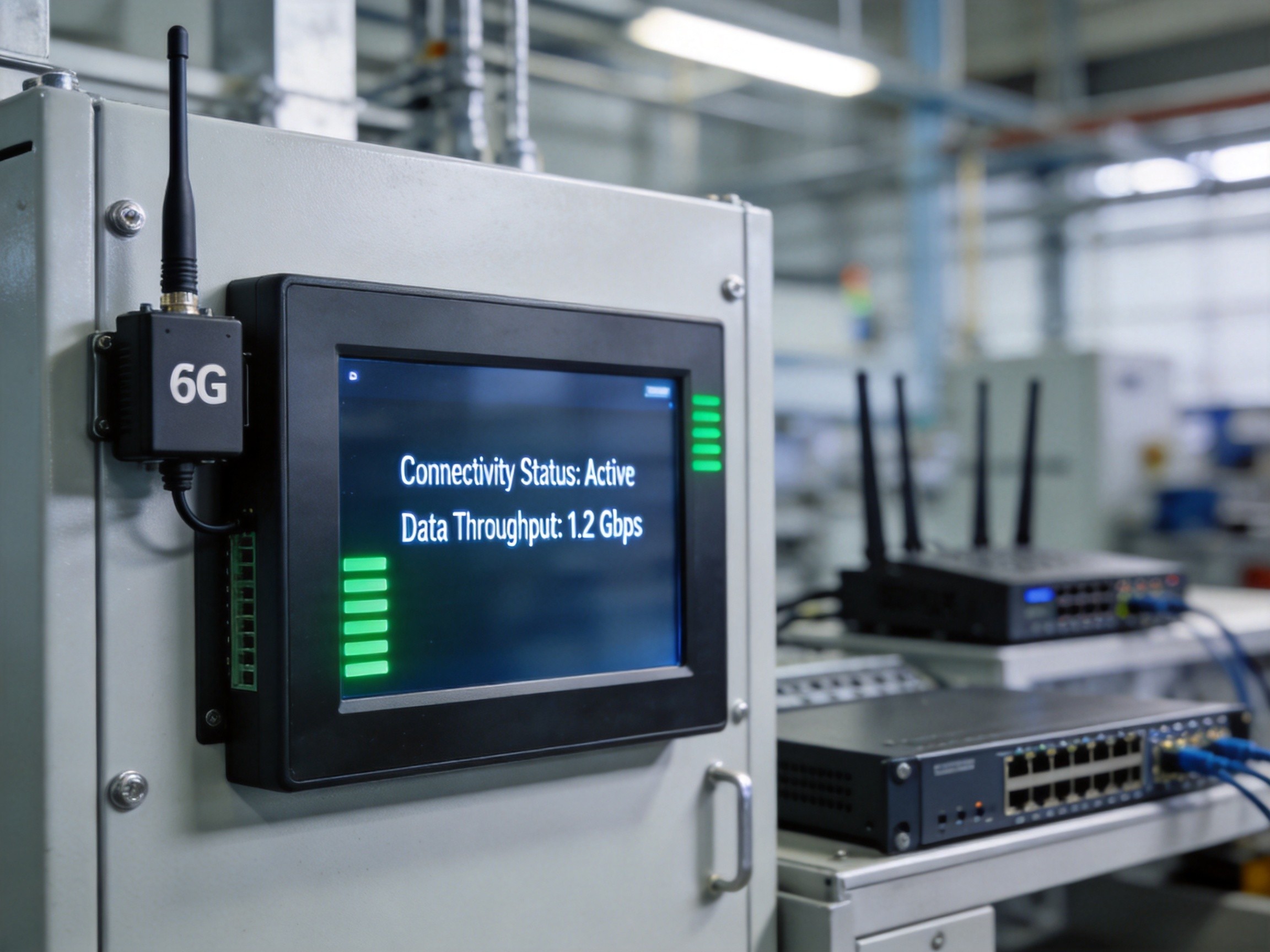
TSMC’s C.C. Wei made a pointed observation during the Q2 2026 earnings call: agentic AI workloads—which involve long-horizon reasoning, tool-call orchestration, and stateful memory management—are driving a resurgence in CPU demand, incremental to GPU and accelerator spending. He noted that x86, Arm-based, and RISC-V CPU architectures are “almost all TSMC’s customers,” meaning the foundry captures the category regardless of which architecture prevails. This CPU renaissance is not limited to the cloud. At the industrial edge, inference workloads are increasingly migrating from centralized servers to on-premise panel PCs, where latency constraints and data sovereignty requirements make local processing non-negotiable. The CPU architectures winning at the edge are not the same ones dominating the data center. They are the ones that can deliver deterministic performance within a 15-watt to 35-watt power envelope, sustain operation across a -20 to 60 degree Celsius range, and remain available on a five-to-seven-year product lifecycle—a requirement that rules out consumer-grade silicon entirely.
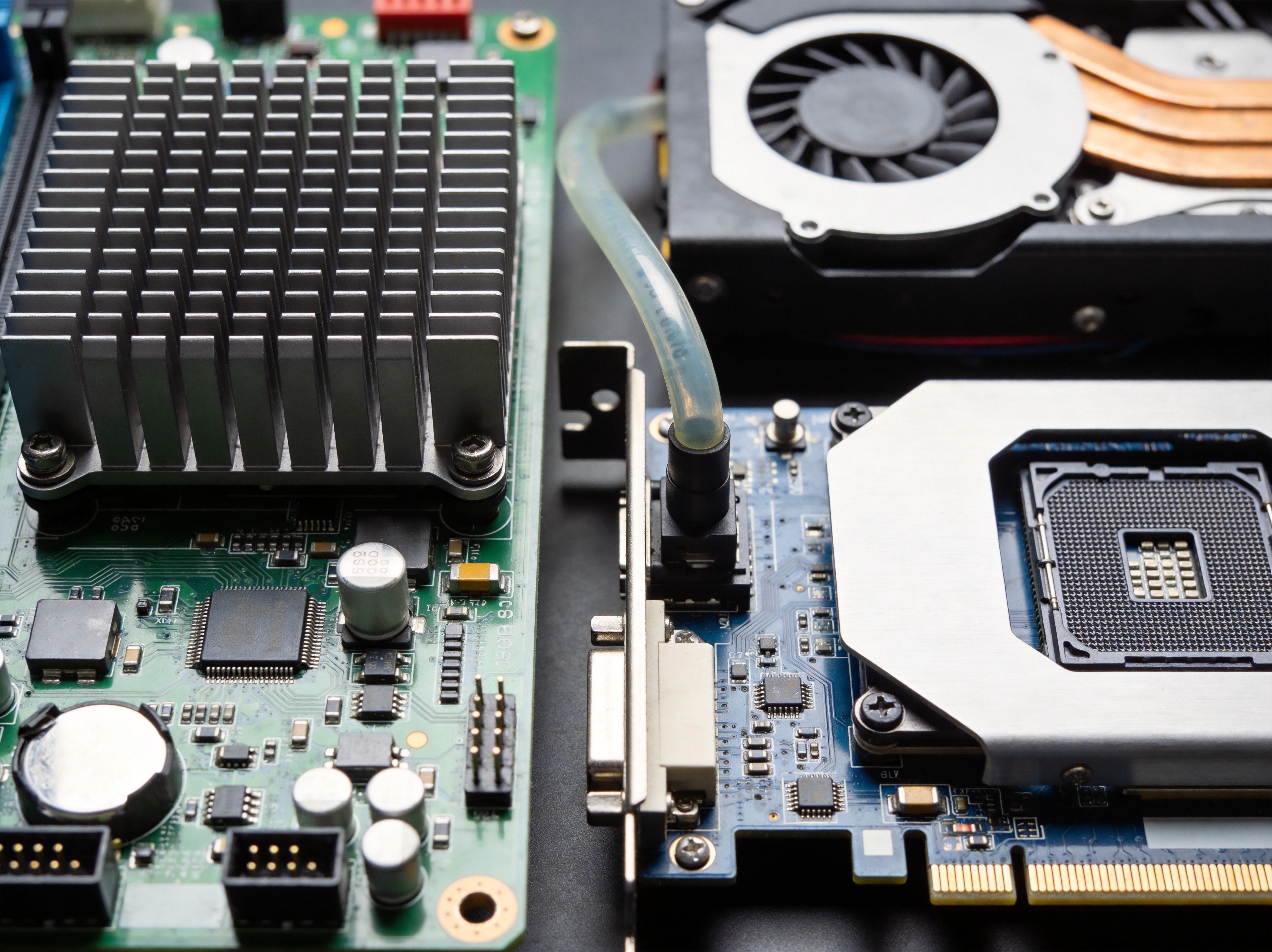
The Silicon Strategy Divergence: Throughput vs. Survivability
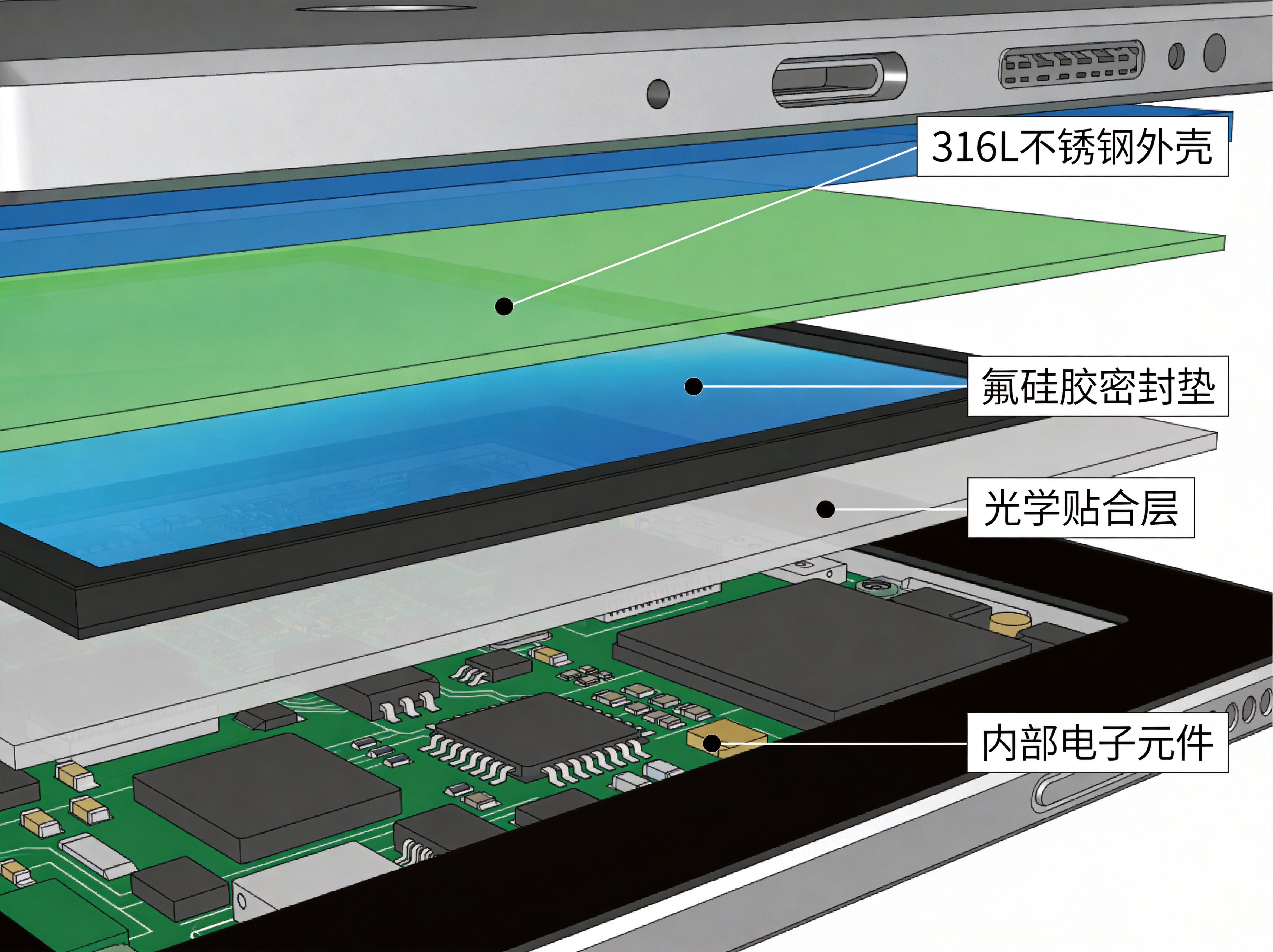
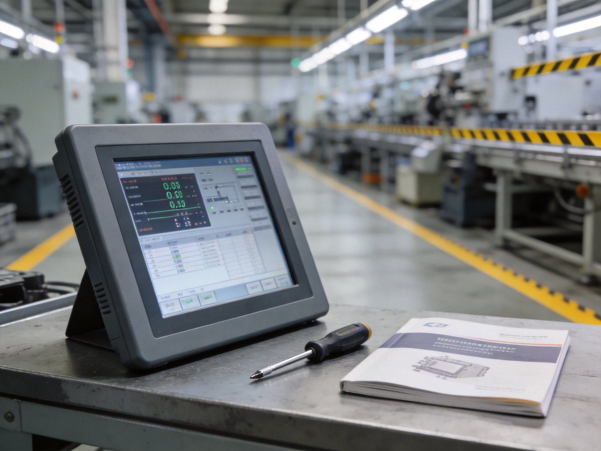
The cloud computing silicon roadmap is optimized for one variable above all others: peak floating-point throughput per watt of electrical power, measured under controlled thermal conditions. The industrial edge roadmap is optimized for survivability: sustained operation under vibration, humidity, dust, and temperature swings that would trigger thermal throttling in a data center processor within seconds. This divergence creates a counterintuitive dynamic: while the semiconductor industry pours hundreds of billions of dollars into 2nm and sub-2nm process development, the most valuable edge computing silicon is often fabricated on mature nodes—28nm, 16nm, or 12nm—where process stability, long-term availability, and proven reliability outweigh raw transistor density. KOXIAN industrial panel PCs are designed around this exact principle, selecting embedded processors that balance adequate compute capability for local inference tasks with the thermal and longevity characteristics that factory-floor deployments demand.
What the TSMC Roadmap Means for Industrial Computing
TSMC’s aggressive 2nm ramp and its $100 billion additional investment in Arizona-based advanced fabs signal that the leading edge of silicon manufacturing will remain concentrated within a small number of consolidated hardware supply clusters for the foreseeable future. For industrial computing buyers, this has two practical implications. First, the processors that power edge panel PCs will continue to be sourced from mature-node capacity that is geographically diversified and less subject to the allocation battles consuming leading-edge capacity. Second, the architectural innovations pioneered at advanced nodes—GAA transistors, backside power delivery, chiplet-based packaging—will eventually trickle down to industrial-grade silicon, but on a timeline measured in years, not quarters. KOXIAN panel PCs are engineered with this reality in mind, using processor platforms that are selected for supply chain stability and lifecycle longevity, not for their position on a marketing roadmap. The right silicon strategy for industrial edge computing is not about chasing the newest node. It is about matching the silicon to the environment where it will spend its operational life—a principle that the cloud computing industry, for all its financial firepower, cannot afford to ignore.
The semiconductor industry is splitting into two distinct worlds: one optimized for peak throughput in controlled environments, the other engineered for sustained reliability under physical stress. Industrial edge computing belongs firmly in the second category, and the silicon strategy that serves it best will continue to diverge from the cloud computing roadmap for years to come.