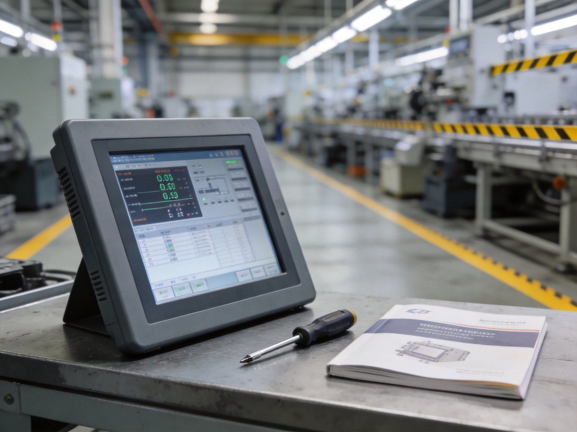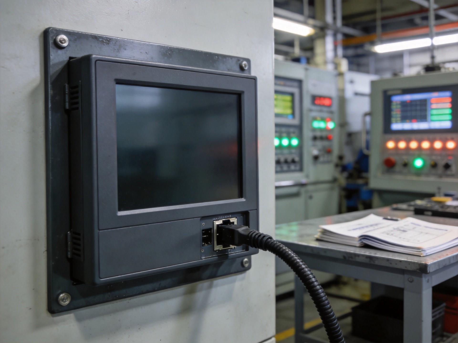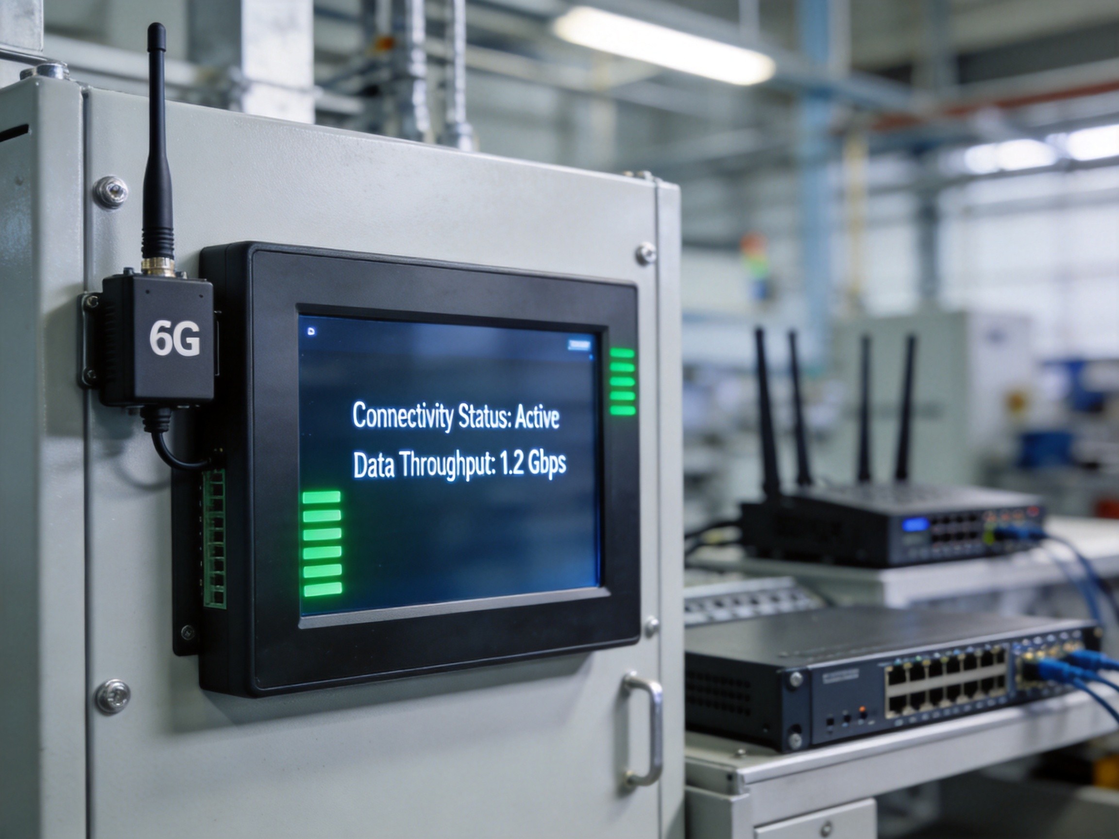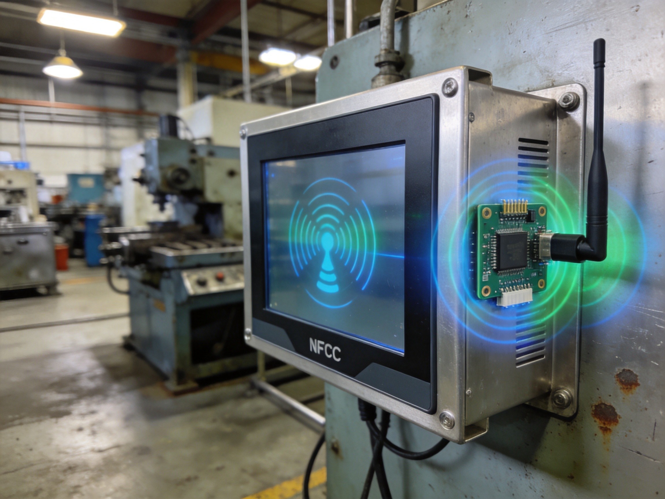
When Samsung and SK Hynix outlined their shared vision for fully autonomous AI-driven fabrication plants by 2030 at a San Jose industry conference in July 2026, the announcement sent ripples beyond the semiconductor sector. The roadmap — built on digital twin simulation, AI agent-based decision-making, and robotic material handling — points toward a future where chip complexity accelerates beyond what monolithic system-on-chip designs can sustain. For industrial panel PCs deployed on factory floors, processing lines, and outdoor terminals, this shift has a direct implication: the era of chiplet-based modular SoC architecture is arriving faster than most system integrators anticipated.
Why Monolithic SoCs Hit a Wall in Industrial Deployments
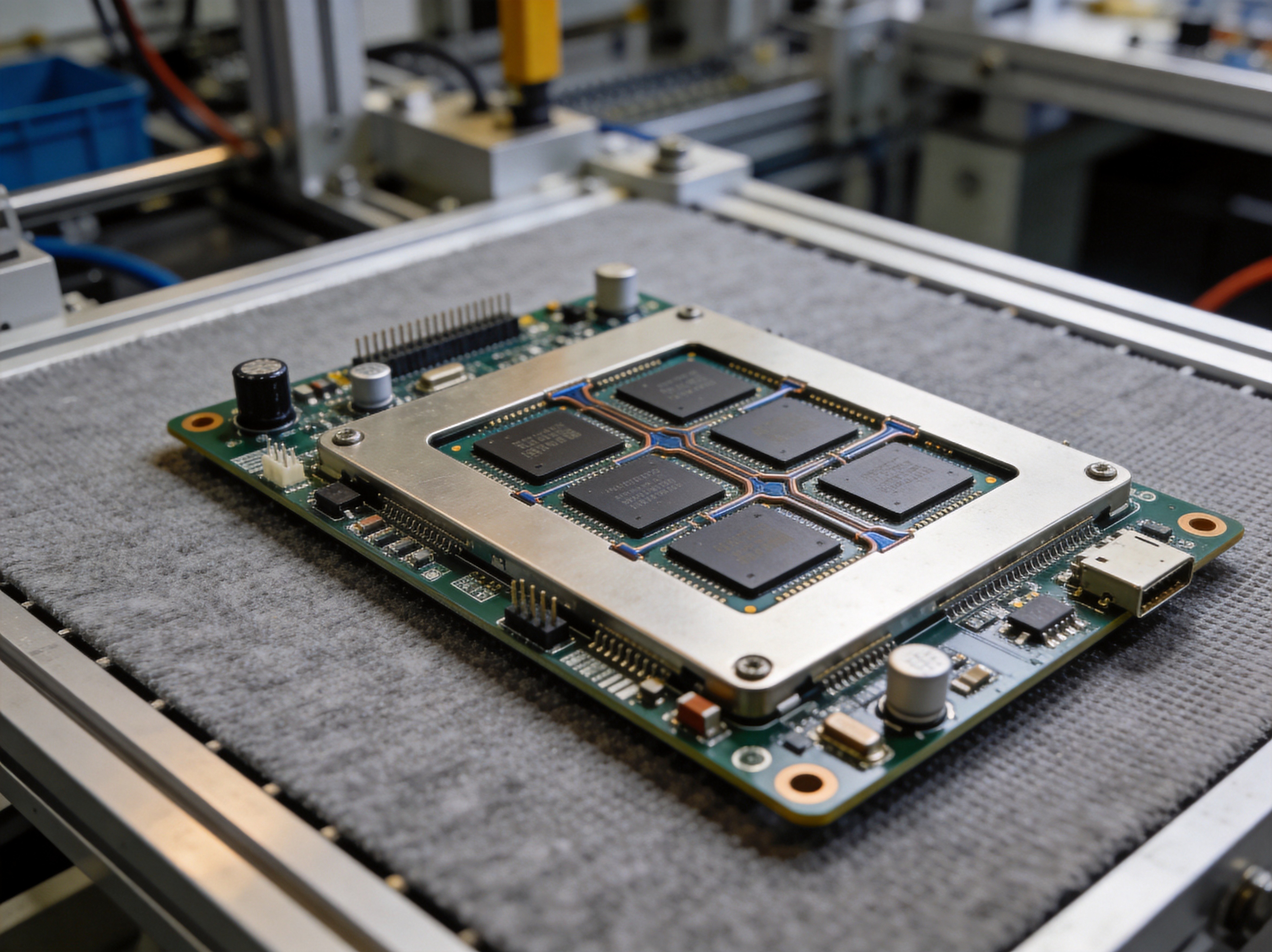
Traditional monolithic SoC design places every functional block — CPU cores, GPU, memory controller, I/O interfaces, and specialized accelerators — onto a single silicon die. While this simplifies board-level integration, it introduces compounding challenges at advanced nodes. Yield rates decline exponentially as die area increases, thermal density becomes harder to manage, and the entire chip must be requalified whenever a single IP block receives an update. For industrial panel PCs operating in harsh environments with wide temperature swings, vibration, and continuous uptime, these constraints translate into longer qualification cycles, higher per-unit costs, and limited flexibility when I/O or processing capabilities need refreshing mid-lifecycle. The economics of monolithic design simply do not scale when fabs push toward sub-3nm geometries.
Chiplet Interconnect Standards and the Industrial Compute Stack
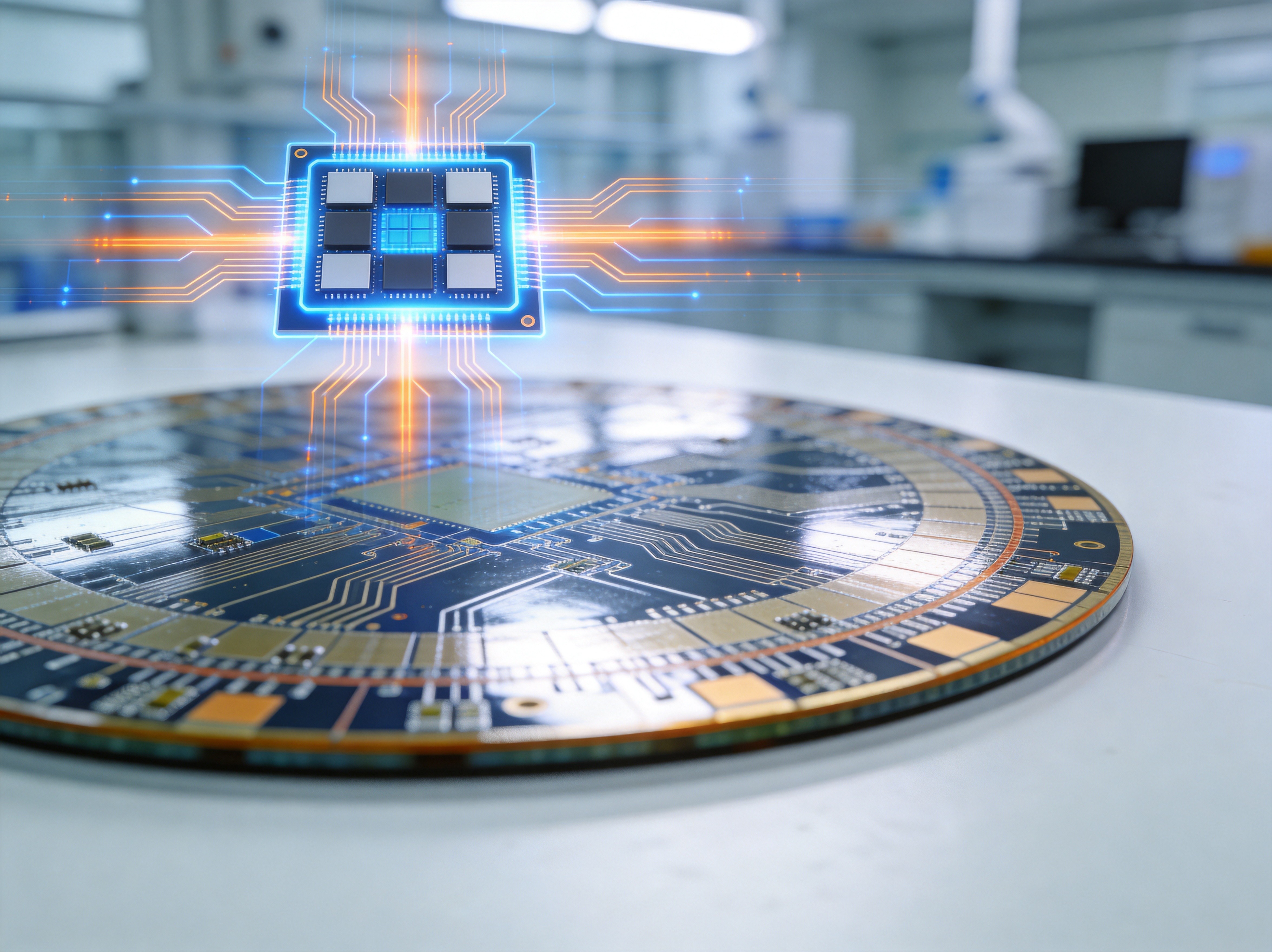
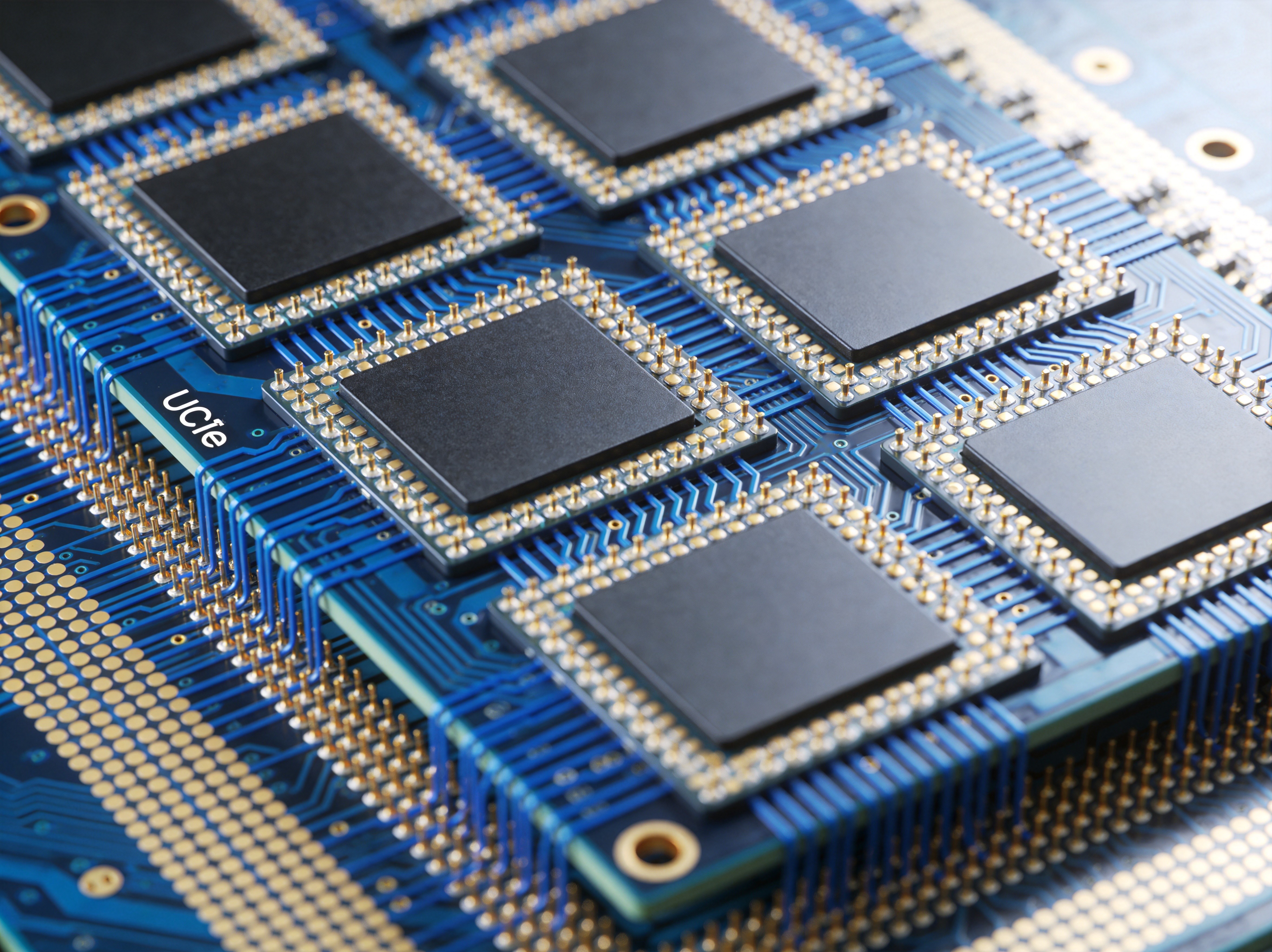
The viability of chiplet architecture in industrial computing hinges on standardized die-to-die interconnect protocols. Universal Chiplet Interconnect Express (UCIe) has emerged as the leading open standard, defining physical layer specifications and packaging options that enable heterogeneous dies from different vendors to communicate over a common interface. For industrial panel PC manufacturers, UCIe-compliant chiplet ecosystems mean pairing a general-purpose compute die with a domain-specific accelerator — such as a real-time vision processing unit or a deterministic networking engine — without redesigning the entire silicon platform. This disaggregation model also allows system builders to source compute dies from one foundry and I/O dies from another, reducing supply chain concentration risk. KOXIAN engineering teams have observed that chiplet-based designs can shorten industrial motherboard qualification timelines by up to forty percent compared to monolithic SoC migrations, largely because validated I/O chiplets can be reused across multiple product tiers without retesting the entire silicon stack.
Thermal and Reliability Implications for Panel PC Deployments
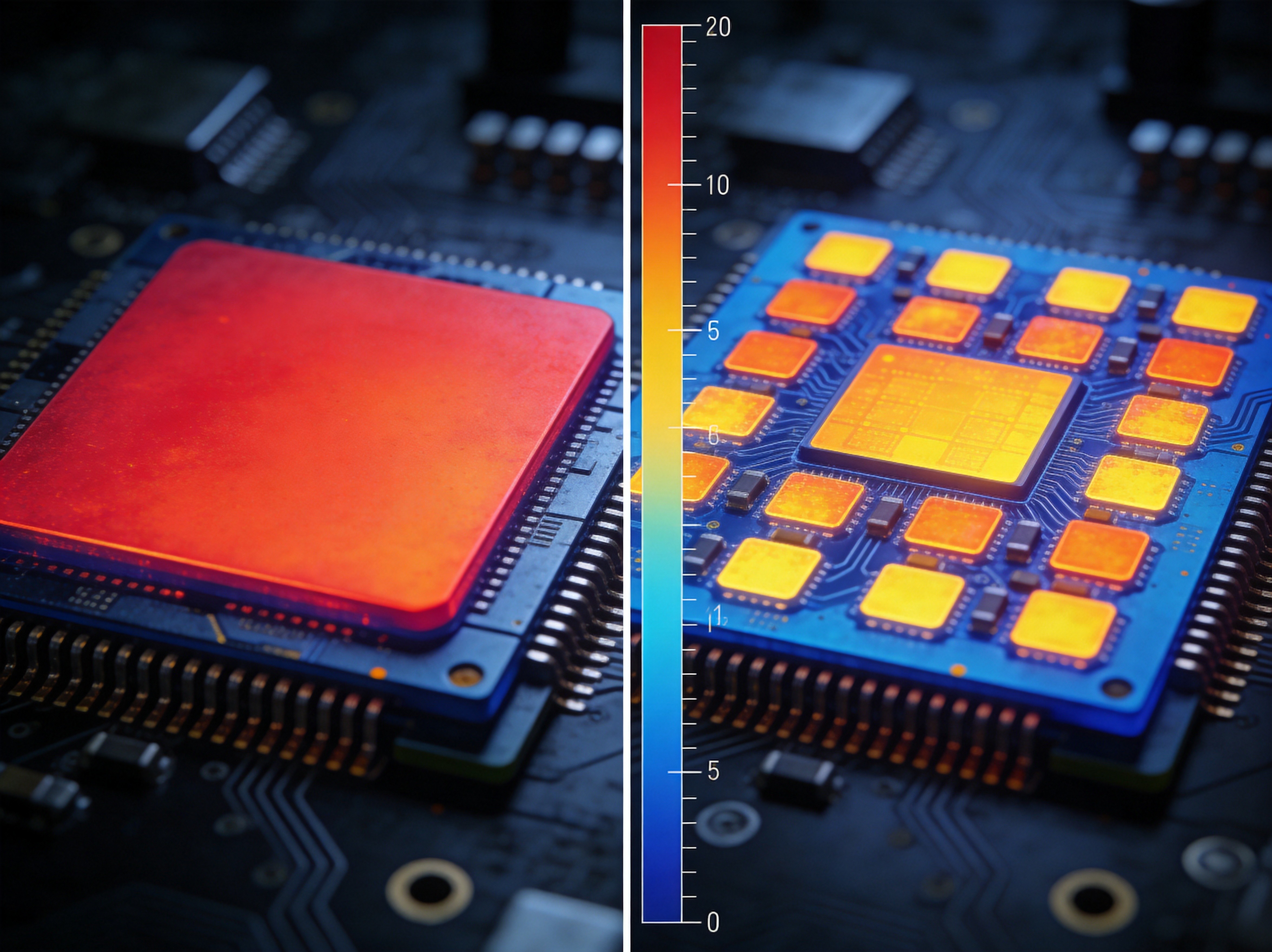
One of the most underappreciated advantages of chiplet architecture in industrial environments is thermal disaggregation. In a monolithic SoC, all functional blocks share the same thermal budget, meaning a hot-running GPU or AI accelerator can force the entire chip to throttle, degrading deterministic performance. Chiplet-based designs distribute heat-generating functions across physically separate dies, each with independent thermal management paths. This is particularly valuable for fanless panel PCs deployed in enclosed cabinets or direct-sunlight outdoor installations, where passive cooling is the only viable thermal strategy. KOXIAN panel PC platforms leveraging modular processor architectures have demonstrated sustained turbo frequency operation at ambient temperatures exceeding sixty degrees Celsius without throttling, a scenario where monolithic equivalents would typically engage thermal protection within minutes.
The AI Factory Connection: What Samsung and SK Hynix Mean for Edge Computing
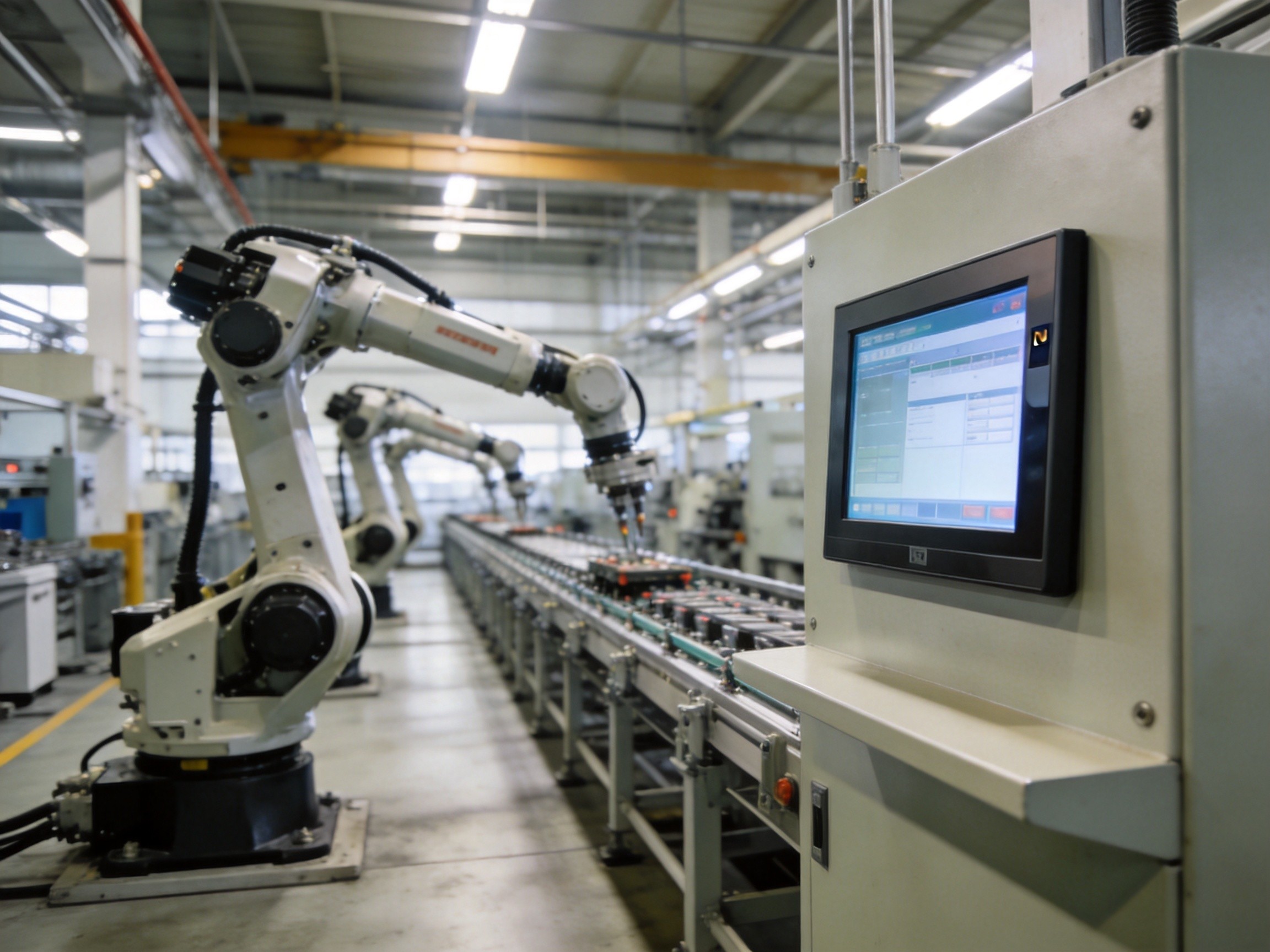
The Samsung and SK Hynix AI factory vision — targeting fully autonomous wafer fabrication by 2030 with digital twin simulation and AI agent-driven process control — signals a fundamental shift in advanced chip manufacturing. AI-optimized fabs promise higher yields on complex multi-die packages, faster iteration on chiplet interconnect validation, and shorter lead times for custom silicon — all directly benefiting the industrial embedded computing supply chain. As these fabrication plants come online, the cost barrier for chiplet-based designs drops, making modular SoC architecture accessible to mid-volume panel PC applications that previously could not justify the packaging investment. For system integrators specifying panel PCs for next-generation production lines, the question is no longer whether chiplet architecture will matter — but how soon their existing monolithic platforms will need to be rearchitected.
The convergence of AI-driven semiconductor manufacturing and modular chiplet design represents a structural shift in industrial computing. As wafer fabs become more automated and capable of producing complex multi-die packages at commercial scale, the panel PC supply chain gains access to processors delivering higher performance per watt, greater functional flexibility, and improved thermal behavior. Forward-looking system architects are already evaluating chiplet-compatible platforms to ensure their roadmaps align with the silicon industry’s trajectory through the end of the decade.